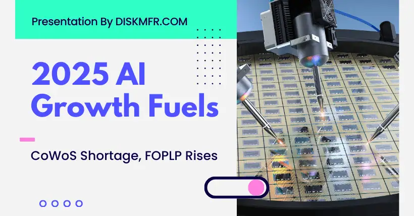
In recent years, the rapid development of AI technology has strongly driven the growth of numerous industries, with the advanced packaging sector being one of them. Recently, industry sources reported that due to the strong demand for NVIDIA’s latest Blackwell architecture GPU chips, the company has secured more than 70% of TSMC’s CoWoS-L advanced packaging capacity for this year. Shipments are expected to grow by more than 20% quarter-over-quarter.
This indicates that the demand for advanced packaging will remain high this year. Although TSMC is actively expanding production, it is still struggling to keep up with the industry’s ever-growing demand, making it imperative to explore new advanced packaging technologies.
01
CoWoS Advanced Packaging Capacity Falls Short, TSMC Accelerates Expansion
With the surge in AI and high-performance computing (HPC) demand, CoWoS technology has become a critical solution. It extends Moore’s Law by integrating chips from different process nodes, enabling accelerated computing while keeping costs under control.
Besides NVIDIA, major international companies such as Amazon Web Services (AWS), Broadcom, and AMD are also competing for TSMC’s CoWoS advanced packaging capacity, resulting in a supply shortage.
To meet the growing market demand, TSMC has been actively expanding its CoWoS capacity over the past two years. According to TrendForce, multiple expansion projects are progressing simultaneously:
- TSMC has acquired Innolux’s factory in Tainan, Taiwan (AP8), with plans for small-scale production by the end of 2025. The facility is expected to reach a monthly capacity of 40,000 to 50,000 wafers.
- The newly constructed AP6B in northern Taiwan received approval for use on December 3, 2024.
- The Chiayi factory, which started construction in May 2024, is progressing rapidly, with its framework already taking shape.
- The AP5B facility in Taichung is expected to begin operations in the first half of 2025.
With these expansion plans, TSMC’s CoWoS monthly production capacity is projected to reach 70,000 wafers by the end of 2025 and exceed 90,000 wafers per month by the end of 2026.
Although recent market rumors suggest that TSMC’s CoWoS orders have been cut by major customers, the company has refrained from commenting. However, the semiconductor packaging and testing supply chain indicates that CoWoS orders remain in short supply, with no order cancellations. The rumors may stem from process upgrades or customers beginning to adopt next-generation fan-out panel-level packaging (FOPLP), leading to misunderstandings.
TF Securities analyst Ming-Chi Kuo also stated that TSMC’s CoWoS expansion plans remain unchanged, with NVIDIA’s planned 370,000 CoWoS wafer orders at TSMC for 2025 showing little change since Q4 2024.
02
FOPLP Gains Traction
Despite TSMC’s aggressive expansion of CoWoS capacity, it is still insufficient to meet market demand. As a result, many packaging and panel manufacturers are seeking alternative solutions. One such emerging advanced packaging technology is FOPLP, which has been linked to the recent rumors of TSMC’s order cuts.
FOPLP is an extension of fan-out wafer-level packaging (FOWLP) technology, using square substrates for IC packaging. This allows for larger package sizes and lower production costs. The key difference between FOPLP and CoWoS lies in the square substrate used in FOPLP, which offers a utilization rate of up to 95%, enabling more chips to be placed within the same unit area compared to circular wafers.
In recent years, companies such as Innolux, ASE Technology Holding, and Powertech Technology have been actively investing in FOPLP. Notably, Innolux has heavily bet on the FOPLP sector and recently launched its “Semiconductor Express Plan,” aiming to cultivate 500 semiconductor professionals through expanded collaboration with industry, government, and academia, with FOPLP as a key focus.
Currently, Innolux has the industry’s largest FOPLP technology with a 700mm x 700mm panel size, targeting mass production in the first half of this year. Meanwhile, ASE Technology is focusing on a 600mm x 600mm FOPLP format, with equipment expected to arrive in Q2 and trial production set to begin in Q3. TSMC is also closely monitoring FOPLP’s development but has not disclosed specific plans regarding size specifications.
03
Challenges Facing FOPLP
The concept of “converting round to square” in FOPLP substrate technology allows panel-level packaging to achieve higher area utilization, increased production capacity, and reduced costs. However, several challenges remain before it can be widely adopted.
The primary challenge is the lack of a standardized panel size in the industry. Unlike wafer sizes, which follow unified standards, different manufacturers have adopted varying panel sizes for FOPLP, requiring equipment adjustments to accommodate different dimensions. This increases design complexity and production costs.
Additionally, the larger panel size compared to traditional wafers introduces issues such as warpage, alignment precision, and process variations. Significant investments in new materials, tools, and methodologies are needed to address these challenges.
Collaboration across the ecosystem is also crucial. Material suppliers, equipment manufacturers, OSAT (outsourced semiconductor assembly and test) companies, and system integrators must work together to overcome technical and economic barriers to facilitate the widespread adoption of FOPLP technology.
04
Conclusion
The rapid advancement of AI technology has significantly increased the demand for advanced packaging. Despite TSMC’s aggressive expansion, it cannot fully meet this growing demand, necessitating the development of new packaging technologies. FOPLP has emerged as a promising alternative, offering scalability and cost efficiency as a replacement for traditional wafer-level packaging. However, its adoption still faces several challenges.
Looking ahead, continuous innovations in materials, equipment, and processes will help FOPLP bridge the gap between cutting-edge performance and manufacturability, positioning it as the industry’s “next big thing.”
Related:

Disclaimer:
- This channel does not make any representations or warranties regarding the availability, accuracy, timeliness, effectiveness, or completeness of any information posted. It hereby disclaims any liability or consequences arising from the use of the information.
- This channel is non-commercial and non-profit. The re-posted content does not signify endorsement of its views or responsibility for its authenticity. It does not intend to constitute any other guidance. This channel is not liable for any inaccuracies or errors in the re-posted or published information, directly or indirectly.
- Some data, materials, text, images, etc., used in this channel are sourced from the internet, and all reposts are duly credited to their sources. If you discover any work that infringes on your intellectual property rights or personal legal interests, please contact us, and we will promptly modify or remove it.


