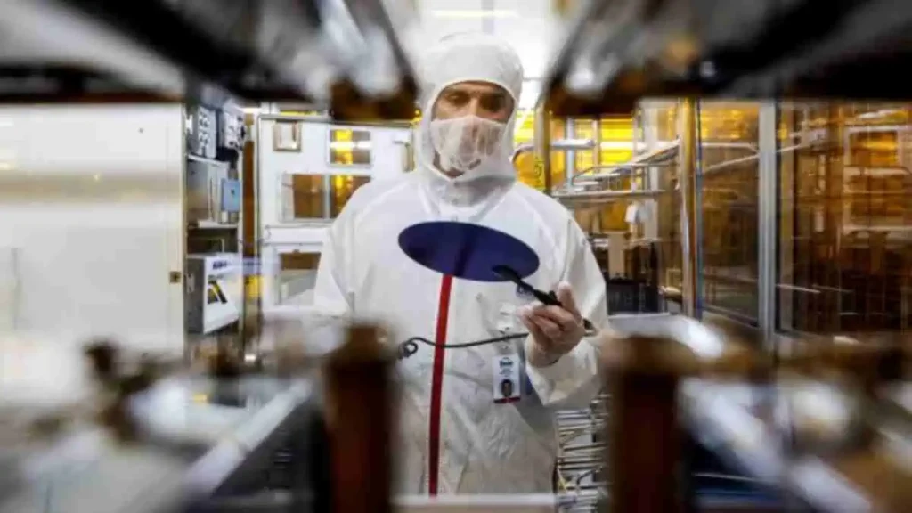
The semiconductor industry is on the brink of a significant transformation as large customers gear up for the mass production of the 2-nanometer process, expected to commence in 2025. This imminent shift marks a pivotal move from the conventional FinFET to the Gate-All-Around (GAA) process. The evolution of this innovative process is set to bring about a profound demand for material analysis in the semiconductor domain.
01
TSMC’s Initiatives in 2nm Production
Taiwan Semiconductor Manufacturing Company (TSMC) stands at the forefront of this technological revolution. With plans to ramp up the production of the 2-nanometer process in 2025, TSMC has secured substantial orders from leading players in various industries, including Artificial Intelligence (AI) and High-Performance Computing (HPC). The anticipation surrounding TSMC’s 2-nanometer technology heralds a wave of future opportunities within the semiconductor landscape.
02
Major Players in the Adoption of the GAA Process
Alongside TSMC, industry giants like Samsung and Intel are also embracing the GAA process. Samsung has already initiated mass production of 3-nanometer wafers using the GAA process. Meanwhile, Intel is on track to commence mass production of GAA-based technology in 2024, symbolizing a comprehensive shift from FinFET to GAA technology in the semiconductor industry.
03
Comparing FinFET and GAA Process Technologies
The transition from FinFET to GAA technology signifies a leap forward in semiconductor innovation. While FinFET technology has served its purpose, limitations in scaling down chip sizes have prompted the adoption of GAA technology. GAA offers significant advantages, such as enhanced control over transistor behavior and reduced power consumption, revolutionizing the way semiconductors are manufactured.
04
Impact on Industries and Technological Advancements
The adoption of the 2-nanometer technology is poised to revolutionize various industries, notably Artificial Intelligence (AI) and High-Performance Computing (HPC). These sectors eagerly anticipate the advancements facilitated by the transition to 2-nanometer technology, foreseeing a surge in computing capabilities and efficiency. The integration of these cutting-edge semiconductors will unlock new possibilities and reshape technological landscapes across multiple sectors.
05
Challenges and Demands in Material Analysis
With the shift towards nano-level technologies, the demand for precise material analysis becomes paramount. Analyzing materials at such minuscule scales presents challenges due to the intricacies involved. The need for accurate and comprehensive material analysis methods becomes imperative to ensure the quality, efficiency, and reliability of the 2-nanometer semiconductor manufacturing process.
06
Prospects and Future Developments in Semiconductor Manufacturing
The transition to the 2-nanometer process represents a stepping stone toward further advancements in semiconductor manufacturing. As the industry pioneers the GAA process, the horizon expands with prospects for future technological developments. The quest for even smaller and more efficient semiconductors beyond the 2-nanometer threshold sets the stage for continuous innovation and breakthroughs in the semiconductor domain.
07
Conclusion
In conclusion, the impending transition to the 2-nanometer semiconductor process, shifting from FinFET to the GAA process, marks a significant leap in semiconductor technology. The anticipated mass production by key players like TSMC, Samsung, and Intel signifies a new era of innovation and possibilities in various industries. The material analysis demands and technological advancements pave the way for a promising future, heralding a transformative phase in semiconductor manufacturing.
08
FAQs
1. What is the significance of the 2-nanometer semiconductor process?
The 2-nanometer process signifies a shift towards more advanced and efficient semiconductor manufacturing, offering enhanced capabilities and performance.
2. Why is material analysis crucial in the semiconductor industry?
Material analysis ensures the quality and reliability of semiconductor manufacturing processes, especially at the nano-level, influencing product efficiency and performance.
3. How does the GAA process differ from FinFET technology?
The GAA process offers improved control over transistor behavior and reduced power consumption compared to the limitations of FinFET technology.
4. What industries will benefit most from the 2-nanometer technology?
Industries like Artificial Intelligence (AI) and High-Performance Computing (HPC) are expected to benefit significantly from the advancements enabled by the 2-nanometer technology.
5. What can we expect beyond the 2-nanometer semiconductor process?
The semiconductor industry foresees continued innovation, aiming for even smaller and more efficient technologies, driving future advancements beyond the 2-nanometer threshold.
Related:

Disclaimer: This article is created by the original author. The content of the article represents their personal opinions. Our reposting is for sharing and discussion purposes only and does not imply our endorsement or agreement. If you have any objections, please contact us through the provided channels.


