Despite the changes, as an NPI engineer, DFM manufacturability analysis covers a wide range of areas. Today’s topic is the production of PCB prototypes.
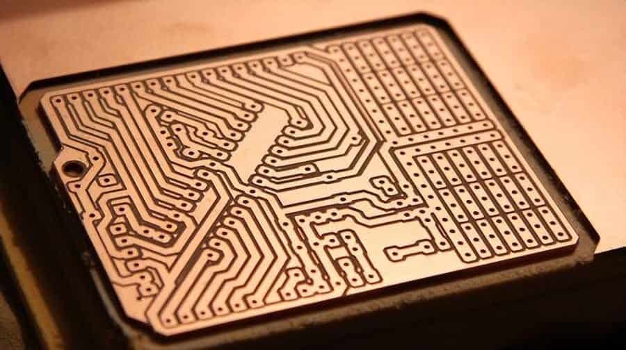
1. What is a PCB Prototype?
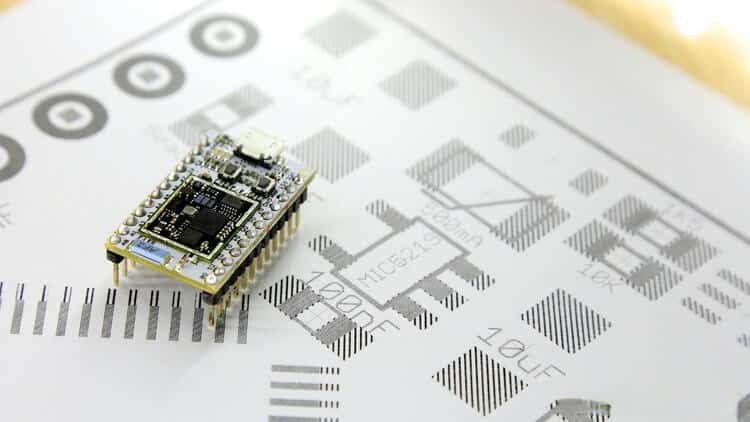
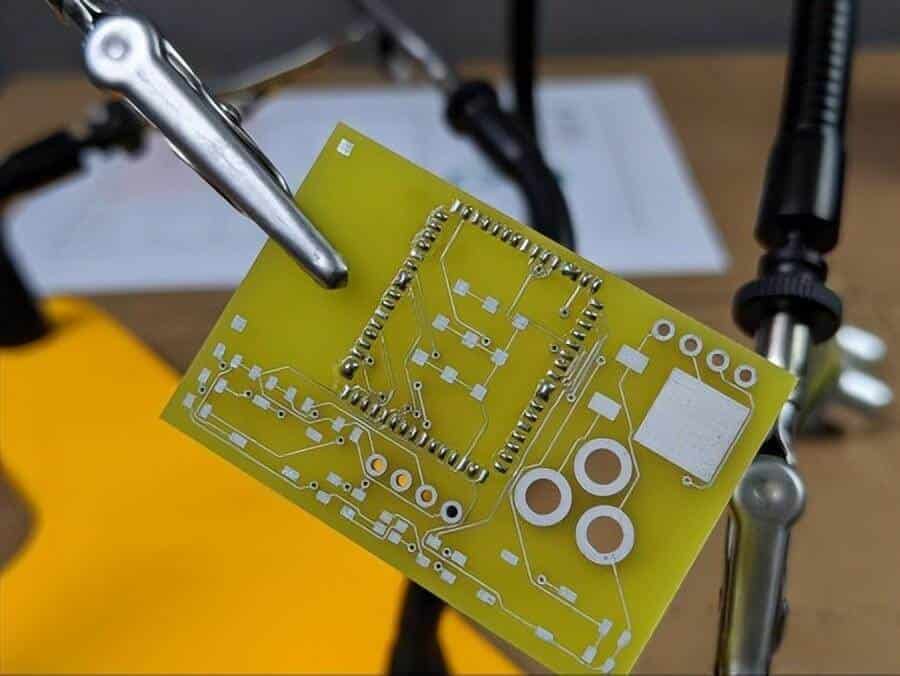
Essentially, a PCB prototype is an early sample of a product created to test design concepts and feasibility. While most prototypes are made to test basic user functionality, a PCB prototype also needs to be functional to some extent because the purpose of PCB prototype production is to test the overall functionality of the design.
During the PCB prototype production process, engineers can experiment with different PCB designs and manufacturing specifications to find the most effective one.

2. Benefits of PCB Prototypes
a. Shorten Time and Save Cost
During the process of designing a PCB, engineers go through multiple iterations before creating the final product, which can result in a lengthy timeline. However, PCB prototypes can help speed up the entire design and manufacturing process in the following ways:
- Complete Testing
PCB prototypes can help PCB design engineers quickly and accurately test design issues. Without this step, discovering design flaws can take more time and if not delivered on time, it may lead to customer dissatisfaction and revenue loss.
- Customers can see the product in advance for better communication
Customers often want to see the product at various points in the production process, and providing prototypes as support can help better convey the design. It can also minimize communication with the customer and reduce the time needed for redesigns requested by the customer.
- Maximize rework reduction
PCB prototype testing allows for viewing and testing of the circuit board before production, reducing rework. If defective products are put into production, it will take more time and cost more in the later stages.
b. Help make manufacturing and production smoother
When using a third-party PCB prototype manufacturing service, it is important to choose a good communicator. There are several things in the design process that can lead to errors, including the following:
- Too many revisions without communication can lead to confusion and difficulty in identifying the best version
In the design process, accumulation and overlap of PCB versions can occur due to changes in clients or design teams, and inadequate documentation can lead to difficulty in identifying versions.
It is also possible to forget the best design in order to meet customer requirements.
- Design blind spots
Designers may be more skilled at designing a specific type of PCB but may have less experience in other areas, which may result in minor issues during the design process.
- Design Rule Check (DRC)
Although DRC tools are very useful for identifying obvious design problems, they also have limitations.
For example, while DRC can verify the existence of a ground return path, it may not be able to determine the best routing geometry, size, and length for the path, leading to suboptimal routing.
All of these issues can result in lower efficiency, design defects, and other problems missed during review by designers. However, some prototype manufacturers have ways to address these issues and can provide design improvement suggestions before producing a prototype, making the PCB prototype more suitable for the testing process.
c. Testing and reviewing the functionality of the product in advance
Having accurate and reliable PCB prototypes can make it easier to address design issues throughout the entire development process. High-quality prototypes represent the functionality of the final product and can help engineers to view and test the following aspects:
- PCB designs
Prototype design can help engineers identify defects early in the development process. The more accurate the design, the more accurate the defect identification will be. This can minimize design costs and shorten project time.
- Functional testing
There are some things that may be effective in theory, but not in practice. Having an accurate PCB prototype can help evaluate theoretical values and check if they appear in the actual values.
- Condition testing
Many products need to be applied in specific environments, so PCB prototypes must undergo appropriate testing to ensure normal operation in these environments.
For example, prototypes often undergo temperature variation testing, power variation testing, and shock resistance testing.
- Design of the final product
PCB prototypes can help determine whether adjustments need to be made to the product or packaging plans for the final PCB design.
For these purposes, an accurate PCB prototype can greatly simplify other processes and help engineers prepare for the production plan.
d. Testing components individually
Engineers often use prototype PCBs for testing, and the most significant use of testing is to test individual components and functions. Prototype PCB testing primarily involves testing a single function integrated into the PCB to ensure that it works as expected. This type of testing can be used for various purposes, including:
- Testing the design theory
Simple PCB prototypes can be used for concept validation, allowing engineers to see and test design theories before further design processes.
Engineers can evaluate whether the design is effective, and if not, identify where the problem lies.
- Decompose complex design
Typically, a simple PCB prototype will break down the fundamental parts of the final PCB to ensure that the design executes a basic function before moving on to the next one.
Gradual testing helps identify design issues in a modular manner, enabling quicker and more precise adjustments. Isolated testing methods can assist engineers in efficiently and effectively testing individual functionalities.
e. Reduce costs
“The standard production and operation costs of PCBs are high, and prototypes are essential for reducing production costs. They can help engineers solve and avoid the following problems:”
- Identify design flaws
The earlier engineers can identify design flaws, the earlier they can rectify them, resulting in lower repair costs. The later the issues are discovered, the higher the repair costs become. If the problems persist until full-scale production, they may exceed the budget.
Through high-quality PCB prototype manufacturing services, design flaws can be quickly and accurately identified and resolved, resulting in cost savings in the long run.
- Determine product adjustments
In some cases, adjustments to the PCB may result in slight differences in shape or material from the original plan, potentially impacting the product’s specifications and manufacturing requirements.
PCB prototyping can determine the need for product adjustments early on, thereby improving planning and reducing the costs of the product and related packaging redesign.
In short, PCB prototyping can help improve product quality while reducing the overall cost of the manufacturing process.
3. PCB prototype manufacturing specifications
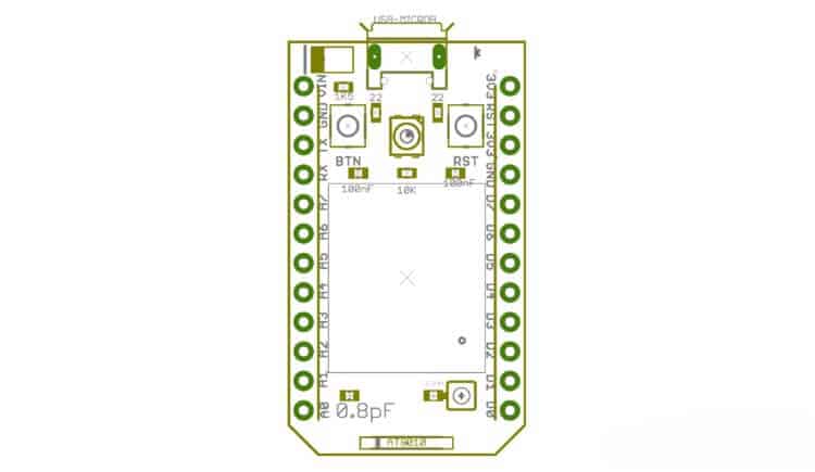
a. Dimensions
This is very simple; it refers to the dimensions of the PCB. The cost of PCBs is proportional to their surface area, so it is essential to utilize space effectively to minimize costs. Similarly, irregularly shaped PCB board designs can result in material waste during the manufacturing process, and smaller rectangular PCB boards within the same board will be more expensive.
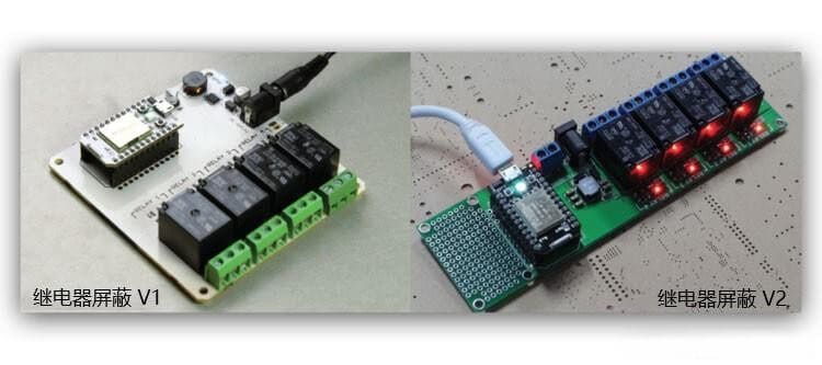
The first version of the relay shield occupied an area close to 74.5 cm^2, with a lot of unused space. The second iteration (prototype!) reduced the footprint by 65.4 cm^2.
b. Layers
The number of layers in a PCB is a fundamental indicator of its complexity. Extra copper layers in a PCB can be thought of as high-speed highways stacked on top of each other. These can be used to route electronic flow between components and pins when their electrical connections overlap.
c. Material Type
Standard multilayer PCBs are made up of several layers of copper-clad boards stacked together. The most commonly used PCB material type currently is glass epoxy resin or the more well-known FR-4, where FR stands for flame retardant and the number represents its flammability.
However, caution must be exercised when designing high-speed or RF boards, as the material’s dielectric properties and thickness are critical.
d. The thickness of a circuit board
PCB manufacturers choose the PCB core size based on the number of copper layers, resulting in the required thickness of the circuit board. If the PCB is enclosed in a tight space, a thickness of 1.0 millimeters or less may be required. Manufacturers can usually accommodate thicknesses as low as 0.4 millimeters.
e. Surface Treatment
Solder pad plating is a technique in which the exposed copper surface of a PCB is coated with another metal material to improve the solderability of the pads during assembly. The most common plating technique is leaded or lead-free HASL (hot air solder leveling), in which the solder is pre-coated onto the circuit board during the PCB assembly process. Another technique is ENIG (electroless nickel immersion gold) plating. This is a more expensive plating technique, but it offers improved oxidation resistance and surface flatness. This makes it an excellent choice for large BGA components and exposed contact pads or test points.
The PCB on the left is plated with ENIG, while the one on the right is standard HASL. Notice how the HASL pads are uneven, while the ENIG pads are completely flat.
f. Impedance control
If a PCB has radio components (such as Wi-Fi or Bluetooth), impedance control may need to be specified. Impedance control means that a specific set of traces (usually in RF networks) presents a known resistance to all signals transmitted through them.
Impedance is affected by several factors, including the dielectric of the prepreg material, trace width, and solder mask layers. Controlling impedance is critical for optimizing wireless antenna performance. For example, Wi-Fi antenna circuits are often controlled to 50 ohms impedance. Impedance control requires expensive equipment and not all manufacturers can guarantee controlled impedance. This can increase manufacturing costs, and if tolerances for controlled impedance are relatively tight, costs can be even higher.
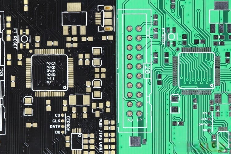
g. Minimum width/spacing
This is a measure of the minimum width of copper traces and the minimum distance between them on a PCB.
The left board uses default width and spacing tolerances, while the right board requires more. Observe how the holes on the vias are not perfectly centered. This becomes a problem when the PCB manufacturer cannot adhere to its tolerances, so it is best to use copper as much as possible.
h. Hole size
This refers to the size of the holes and vias (vertical electrical connections established between copper layers) on a circuit board. Specifying small pads and vias on a PCB is a good way to save space, but it can also make manufacturing more difficult. Smaller holes mean tighter tolerances during the drilling process and can result in more scrap material.
i. Solder Mask Layer
A solder mask layer helps prevent solder bridges and potential short circuits by being applied over the copper traces of a PCB. In addition to the standard green color, you can also choose from red, yellow, blue, black, or white.
The image below shows a pre-production sample where discoloration occasionally occurs during high-temperature reflow soldering and wave soldering steps. The final decision was to switch to a black solder mask layer to avoid costs associated with cosmetic defects.
The pink discoloration on the white solder mask layer on the left is caused by residual chemicals in the PCB manufacturing process and high temperatures during reflow and wave soldering. The sample on the right is a normal one.
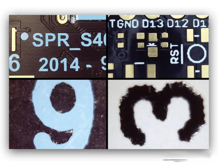
j. Silk Screen Printing
Silk screen printing is used to record and annotate text, graphics, and symbols on PCBs. A more precise alternative to silk screen printing is LPI printing (Liquid Photo Imaging), which can create silk screen printing with much higher resolution at a slightly higher cost.
The comparison between LPI (left) and traditional silk screen legend printing (right) at the same magnification.
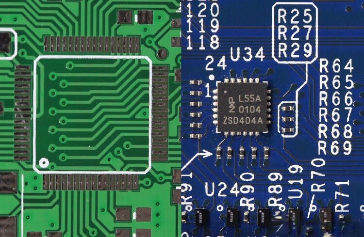
k. The minimum spacing
In the PCB field, “spacing” refers to the distance between adjacent pins on electrical components.
If a PCB requires a complex part with a large number of pins and very fine spacing, a higher-cost assembly factory may be needed.
Spacing that is too narrow often results in decreased yield, so the expected cost of scrap (expected scrap rate % * scrap cost) needs to be considered.
Modern integrated circuits now offer nearly infinite numbers of packages and spacings. QFN and BGA packages are often more challenging when making prototypes or hand-assembling PCBs.
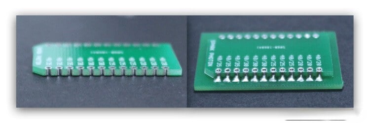
l: Slotted Hole
If you have a template or PCB that will be manufactured and installed onto another PCB, you may consider adding castellated pads to the PCB design.
The image on the left shows a PCB with castellated pads. Note the HASL copper plating (silver) on the side of the PCB. The image on the right shows the PCB installed onto a host board.
m. Restriction of Hazardous Substances (RoHS)
If you are producing PCBs, you should communicate your requirement for RoHS compliance to the manufacturer. While it is a common requirement, leaded and non-compliant components are still prevalent, so without clear specifications, they may sneak into the design.
The above is some knowledge about PCB prototype manufacturing. I hope everyone can support me and leave comments in the comment section for discussion and exchange.

Related Reading:


