Witness the changes in the chip giant over the past fifty years as Silicon Valley’s ‘soul’ museum takes you on a firsthand journey.
On September 21st, Relevant media reported from San Jose that the 2023 Intel On Technology Innovation Conference opened on September 19th, local time, in San Jose, California, USA. On the eve of the summit, under a clear sky with sunlight pouring over Intel’s headquarters campus, Relevant media and global media came to visit the Intel Museum.
The Intel Museum was first established in the early 1980s and opened to the public in 1992. It underwent expansion in 1999 and added a shopping mall, occupying 10,000 square feet. If you happen to be in San Jose, take some time to visit here, follow the exhibits through the space-time corridor, and go back to the place where modern technology began. See the figures, technologies, chips, papers, newspapers, and allusions that changed the world. See what the super-clean, highly automated silicon chip factories look like and how sand turns step by step into the world’s most sophisticated and complex machines.
Here, we not only commemorate Intel’s glory but also record its past failures. There are interesting historical materials that will make you smile, rich chip science knowledge, and many interactive experiences designed for students to learn while having fun, such as writing your name in binary and quickly sliding on sensors to measure your hand speed. I believe most technology enthusiasts will gain a lot from this.
01
The ‘Three Giants’ of Intel Shaping the Chip World
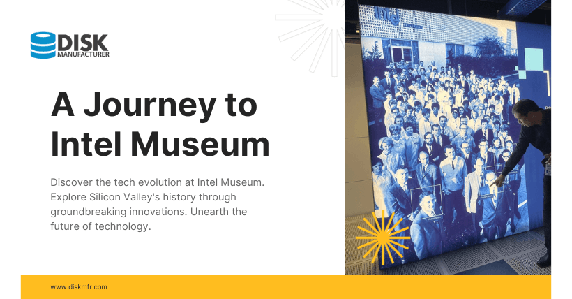
Entering the exhibition area, the first thing that catches your eye is a photograph on the left-hand wall. This is a picture of 106 Intel employees gathered outside the former Santa Clara factory in 1969.
Standing at the front row are two individuals, Intel’s co-founders Robert Noyce and Gordon Moore. Noyce is looking directly at the camera, while Moore gazes into the distance. Intel’s future CEO, Andy Grove, can be seen in the second row, farthest to the right, wearing glasses with his hands in his pockets. It was these three individuals who pioneered a new era in computer memory chips, leading to a wave of innovations, including Intel’s first microprocessor, which ignited the computer and internet revolution. In this photo, there is also a young man wearing glasses with his eyes closed. Although not highlighted, he is a figure destined to make history – he invented Intel’s first CPU.
Returning to the story of Intel’s founding, we need to go back to a spring afternoon in 1968 when Bob Noyce was mowing his lawn at home, and Gordon Moore came to visit. Moore suggested that the emerging technology of semiconductor memory could serve as the foundation for a new company. Shortly thereafter, on July 18, 1968, the two officially established Intel in Mountain View, California. Andy Grove later joined them. Before settling on the final name for Intel, Moore and Noyce considered several name combinations.
Initially, Intel’s name was “NM Electronics,” combining the initials of Noyce and Moore. Since Noyce was two years older than Moore, his initial came first. However, they soon decided they preferred another name – Intel, derived from “Integrated Electronics.” Ultimately, they purchased the right to use the Intel name in a business deal with a chain hotel in the Midwest. Moore recalled, “We thought it was easier to pay $15,000 than come up with another name.” Noyce was Intel’s first employee, Moore the second, and Grove the fourth. Grove always jokingly claimed he should be the third employee because when the company was officially registered, he just missed being the third; the actual third employee was an Israeli named Wiedschen. The reason Intel later established a factory in Israel was related to Wiedschen because when he retired and returned to Israel, he asked Grove for money to start a factory there. This is how Intel became one of the largest foreign companies in Israel.
02
Fairchild’s ‘Traitorous Eight,’ Moore’s Law, and the Rise of Silicon Valley
Among the three key figures who laid the foundation for Intel, Noyce was the soul, Moore was the visionary, and Grove was the executor. In 1955, the “father of the transistor,” William Shockley, left Bell Labs and founded Shockley Semiconductor Laboratory. Many talented young scientists were drawn to work with him, including Noyce. However, Shockley, despite being a scientific genius, was not a good manager. When disagreements arose within the team, he didn’t opt for communication but instead assigned tasks to different teams. What was particularly criticized was his lack of trust in his employees. For instance, when one employee had a cut in the lab, Shockley insisted there was a saboteur within the company and even subjected all employees to lie detector tests.
Shockley’s erratic behavior, coupled with the lack of notable products from his laboratory, left team members increasingly disillusioned. Eight of them decided to resign together and founded Fairchild Semiconductor in 1957. These eight individuals became the famous “Traitorous Eight” of Silicon Valley. Their resignation letters were submitted to Shockley on September 18, 1957, a day later referred to as one of the “Ten Days that Shook the World” by The New York Times. Noyce was a highly respected leader among them and was elected as the leader of the “Traitorous Eight.” Under Noyce’s astute leadership, Fairchild grew rapidly and gained fame for inventing the integrated circuit. In 1965, Gordon Moore, one of the “Traitorous Eight,” introduced a concept that continues to influence the information age to this day – Moore’s Law – in a short 3-page paper.
By 1967, Fairchild’s revenues approached $200 million. However, a crisis was brewing. Its parent company continually siphoned off Fairchild’s profits to invest in other businesses, leading to another exodus of the “Traitorous Eight.” Moore and Noyce were among the last to leave, founding Intel and bringing Grove with them. As key talent departed, Fairchild’s fortunes declined, and it was eventually sold. The talents who emerged from Fairchild dispersed like dandelion seeds, contributing to the rise of Silicon Valley. The book “The Silicon Valley Edge” published in the 1980s noted, “About half of the approximately 70 semiconductor companies in Silicon Valley are direct or indirect descendants of Fairchild.” Noyce, often regarded as the “father of Silicon Valley,” was not only a brilliant scientist but also a skilled diplomat and strategist. He held the longest tenure as Intel’s leader and received numerous awards, including the National Medal of Science in 1979, the National Medal of Technology in 1983, and the Charles Stark Draper Prize in 1989, underscoring his immense importance to the industry.
In the 1980s, Japan’s semiconductor industry surged ahead, causing devastation in the American semiconductor sector. Under the relentless lobbying of Noyce and others, the U.S. government recognized the importance of the semiconductor industry to national security and initiated a dumping investigation into Japanese chips.
03
First Product, First Order, First Logo
When Fairchild was founded, the chips they produced didn’t have fixed functions; they were customized based on customer requirements. However, when Intel was established, its founders aimed to create sustainable chips with predefined functions. The earliest such chips they ventured into were memory chips.
Before Intel ventured into memory chips, early storage was done using magnetic core memory. Wires would go in from one end, and pass through the magnetic core, and when two wires had a current simultaneously, it would magnetize the core, turning it into a “1.” Reversing the direction of the current would demagnetize it, making it a “0.” There was also a diagonal wire to read “0101.”
The principle of this technology was simple in theory but incredibly complex to manufacture. Many female workers had to delicately assemble it, and any mishap like chipping the insulation could lead to short circuits. This manual production process was costly, considering the limited storage capacity. Intel, however, used the principle of transistor switches with an added capacitor to store “0101,” which proved to be a more cost-effective solution.
In simple terms, how a chip functions depends on how its transistors and gates are designed. Transistors act as switches, allowing or blocking the flow of current. Gates control these transistors, enabling the flow and reception of current and processing digital signals (0s and 1s) into commands and information. Intel was founded in July 1968, and it didn’t sell any products that year, incurring a loss of $446,000. However, it turned profitable in 1969, with sales reaching $565,900. From then on, Intel only reported losses for one year, which was in 1986 due to fierce competition in the memory business from dominant Japanese companies.
In the years 1968 to 1969, Intel achieved several milestones: they introduced their first product, the 3101 Static Random-Access Memory (SRAM) chip, received their first order from Hamilton Electric, and unveiled their first logo.
If the first product, the 3101, showcased Intel’s competitiveness in existing technology, its second product, the 1101, demonstrated its ability to pioneer new technologies that would transform the entire industry.
Intel’s 1101 Static Random-Access Memory (SRAM), released in 1969, was the first commercial chip to successfully implement two critical technologies: metal-oxide-semiconductor and silicon gate technology. These innovations reduced the production cost, improved quality, and increased the production efficiency of integrated circuits, paving the way for lower-cost computers and ultimately personal computers (PCs).
In that same year, Intel began manufacturing chips on silicon wafers with a diameter of 2 inches (50 millimeters). Subsequently, the size of their wafers and their production efficiency continued to increase, reaching 12 inches (300 millimeters). It was also the year when Intel introduced its very recognizable first logo, featuring a slightly tilted “e.”
04
The Birth of the First Personal Computer and CPU
On November 15, 1971, Intel introduced its first microprocessor, the 4004. Intel’s 4003 was a printer interface, the 4002 was RAM, and the 4001 was ROM program storage.
The programmable 4004 was the first general-purpose processor on the market, and it’s from here that the x86 architecture originated.
The first-generation CPUs were tailored to specific manufacturers’ requirements. The second generation took a significant leap with the 8008, which doubled the capabilities. However, it was the 8080 that many consider the first true general-purpose microprocessor. The 8080 had 4,500 transistors and could perform 29,000 operations per second, which was 20 times faster than the 4004.
Subsequently, the 8088 and 8086 were released simultaneously, with the former being 8-bit and the latter 16-bit. The next generation included the 80186, which was a transitional product, followed by the 80286, 80386, and 80486. After that, Intel moved away from this naming convention and entered the “Pentium” era.
The Altair 8800, invented by American computer enthusiast Edward Roberts, is widely recognized as the world’s first microcomputer. Users programmed it by flipping switches. It used the Intel 8080 microprocessor and was sold for $439. Thousands of these were purchased by electronic hobbyists for assembly at home.
Intel’s growth was significantly influenced by IBM. IBM aimed to launch a personal computer (PC) within a year and sought Intel for chips. They also approached Microsoft, but initially, Microsoft didn’t develop DOS; it was created by two professors. IBM convinced Microsoft to buy the rights to the program and provide improvements and support. Intel faced different demands. IBM presented them with three stringent conditions: 1) Provide the technology to another company for free, ensuring IBM had an alternative supplier. 2) IBM should have a 20% stake in Intel. 3) IBM, which had its semiconductor manufacturing facility, wanted the rights to Intel’s technology and chip production.
The company that Intel “gifted” its technology to was AMD (Advanced Micro Devices). AMD’s founder, Jerry Sanders, had previously been a key player at Fairchild, with Noyce overseeing operations and Moore in charge of research and development. Intel’s technology strength can be attributed to Moore, who, upon leaving Fairchild, recruited many of his colleagues to join Intel. This contributed to the decline of Fairchild a few years after Intel’s founding. Sharing was inevitable, so why not make it cheaper for former colleagues? Intel shared its technology with AMD, and in the early days, AMD didn’t need research engineers but instead studied what Intel had done and then went into production. Typically, they entered the market about 1 to 1.5 years later than Intel. Hence, it can be said that AMD was initially nurtured by Intel.
In the 1980s, when Intel faced a crisis, IBM, due to a lack of confidence in Intel, secretly sold its Intel stock. However, the situation soon turned around, and Intel embarked on its most prosperous period in the 1990s, with its stock soaring multiple times each year. It’s unclear whether the decision-makers at IBM, who sold their stock, ever regretted not holding onto it when reminiscing about this matter. This contract expired at the end of 1992. The Pentium processor was introduced in 1993 after the contract had expired.
So, why didn’t Intel continue using numbers to name its processors? It’s because numbers couldn’t be trademarked. Intel gave all employees the chance to participate in naming processors, and the name Pentium was the result of combining ideas from a couple of employees. “Penta” means “five” in Greek, and “ium” typically appears at the end of chemical elements. IBM positioned Intel as a “materials company” providing materials for the entire high-tech industry. Intel’s extensive advertising efforts helped Pentium become one of the “Top Ten Brands” within a year of its launch.
05
The First Failure
The museum also features a special exhibit, which is the artwork created by painter Nagel for Intel’s advertisements. Nagel’s work had a distinct style of high-fashion graphic art that was both idealistic and boldly futuristic, aligning well with the style of Intel’s chip engineering. Intel commissioned him to create many advertisements.
In 1984, Nagel tragically passed away at the young age of 38. By that time, his art had become highly valuable. The abrupt end to his short career made his original artwork created for Intel even more precious, and Intel became the largest owner of Nagel’s genuine works. From the beginning, Intel has been dedicated to connectivity, from early involvement in inventing USB to later developments in 3G, 4G, and 5G technologies.
However, Intel’s first failure was in the realm of electronic watches. When Intel entered the market, electronic watches were selling for as much as $200. Yet, within a little over a year after Intel’s entry, the prices of electronic watches had plummeted to just over ten dollars. Intel’s substantial investment did not yield the expected returns, and this venture proved to be a costly mistake. Moore, in particular, continued to wear one of these watches on his wrist as a reminder that in the high-tech industry, one could easily incur losses with a single misstep.
06
Unveiling Intel Chip Factories and the Semiconductor Manufacturing Process
The model you mentioned represents an Intel factory. The factory’s practical space is quite compact, mainly consisting of cleanrooms.
Air is drawn from beneath the floor, filtered, and then sent downward. The airflow must be strictly vertical because even a slight tilt can lift dust particles. People inside the cleanrooms have to walk very slowly to prevent stirring up dust.
The air in these cleanrooms is replaced every 7 seconds. The rooms are maintained at positive pressure, meaning that if there’s a crack or opening, the air would flow out, preventing contaminants from entering. Silicon is an ideal material for semiconductors because it is abundant in nature. Silicon dioxide is a key component of sand.
Intel purchases blank wafers made from naturally occurring semiconductor silicon. Semiconductors can either conduct or block electrical current depending on how they are processed.
Upon receiving wafers, the first step involves oxidizing them with high-purity oxygen to insulate the surface. A photosensitive material is then applied, like the material used in photography development. Through ultraviolet exposure, layers of this material are etched, and silicon is deposited layer by layer. This process is used to create transistors. For 8-inch silicon wafers, the container used to melt the silicon was originally made of germanium. However, germanium’s melting point is 937 degrees Celsius, which makes it unstable in high-temperature environments like deserts. Silicon, on the other hand, has a melting point of over 1400 degrees Celsius and is more stable. In the early days, finding a suitable container for melting silicon was challenging. Eventually, they started using silicon itself. The container had an electric heating coil, and the entire container was made of silicon. Inside, a thin silicon ingot was slowly rotated and lifted, gradually forming a single crystal of silicon. Single-crystal silicon has extremely high purity, reaching 99.999999%.
Why is such a high level of purity necessary? Another step involves rotation. The container rotates, and as the silicon ingot cools and is lifted, its rotation helps eliminate impurities. The silicon ingot is a large single crystal, and it’s trimmed and ground to a uniform diameter. It can be sliced into 12-inch silicon wafers and weighs 122 kilograms, approximately the weight of two adults.
After creating the single crystal silicon, it needs to be cut. Laser cutting would destroy the wafer, so mechanical cutting is used. In the past, for wafers below 12 inches in diameter, diamond grit saws were used. However, these saws became blunt after cutting a few wafers, so now wires filled with diamond grit are used for cutting. Each wire can only be used twice before becoming ineffective. Silicon itself is an inexpensive element, but the processing costs are high, making semiconductor manufacturing expensive. Next to the silicon ingot exhibit, there is a large model of an Intel factory. According to the information provided, the first thing they do when constructing a factory is to build a concrete factory, and after that, they dismantle the concrete factory to create a parking lot. All the water used in Intel’s factories is recycled.
07
Conclusion: “Passing the Torch of Innovation in Semiconductors,” Changing the World
After taking a tour around, the rich and multifaceted history of this legendary semiconductor giant, along with the invaluable technological treasures it has bequeathed to the world, are vividly displayed before the audience. When you witness the painstaking complexity of early chip design processes, the birth of many “world’s first…” chips, and the evolution of single chips accommodating increasingly larger transistors with technological advancements, it’s hard not to be in awe of the history written and miracles created by Intel. Due to limited time, this tour only scratches the surface, and the breadth and depth of the museum’s exhibits are far richer than what this article presents. The charm of the museum lies not only in commemoration but also in the continuity. It’s a testament to the ongoing innovation and courage of pioneers, the resilience and adaptability in the face of failure, and the enduring power of chips to change the world, from the past to the present and into the future, passed down through generations, always burning bright.
Related:

Disclaimer: This article was created by the original author (ZeR0 from Xindongxi). The content of the article represents their personal opinions. Our reposting is for sharing and discussion purposes only and does not imply our endorsement or agreement. If you have any objections, please contact us through the provided channels.
Author: ZeR0


