When hardware engineers first come into contact with multi-layer PCBs, it’s easy to feel dizzy. Often consisting of ten or even eight layers, the circuits resemble a spider’s web.
I have drawn several diagrams illustrating the internal structure of multi-layer PCBs, using three-dimensional graphics to display various layered PCB internal architectures.
01
The Core of High-Density Interconnect (HDI) lies in vias
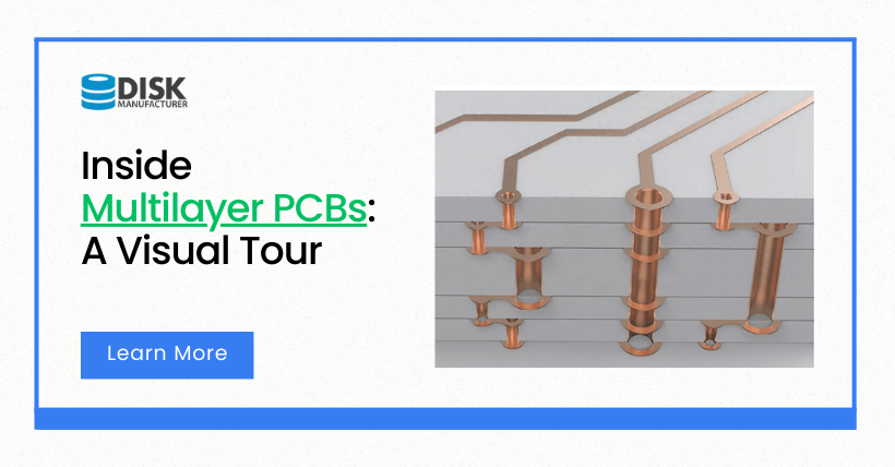
The processing of circuitry in multi-layer PCBs is not significantly different from that in single or double-layer PCBs. The most significant difference lies in the process of vias.
Circuit traces are typically etched onto the board, and vias are created by drilling holes and then plating them with copper. These processes are well understood by hardware developers and need no further elaboration.
In the realm of multi-layer circuit boards, you’ll commonly encounter the following types: through-hole boards, single-layer HDI boards, double-layer HDI boards, and two-layer stacked HDI boards. Higher-order boards like three-layer and arbitrary-layer interconnect boards are less commonly used due to their high cost and won’t be discussed extensively here.
In general, 8-bit microcontroller products typically employ 2-layer through-hole boards, while 32-bit microcontroller-level smart hardware uses 4 to 6-layer through-hole boards. For Linux and Android-level smart hardware, 6-layer through-hole to 8-layer single-layer HDI boards are common. Compact products like smartphones often utilize 8-layer single-layer to 10-layer two-layer circuit boards.
02
The Most Common Through-Hole
There is only one type of via hole, from the first layer to the last layer. Whether it is an external circuit or an internal circuit, the holes are drilled through, called through-hole boards.
Through-hole boards are not related to the number of layers; even two-layer boards commonly use through-holes. Many switches and military-grade circuit boards, which can have up to 20 layers, still use through holes.
The process involves drilling the circuit board with a drill bit and then copper-plating the holes to create a pathway.
It’s worth noting that the inner diameter of through-holes typically comes in 0.2mm, 0.25mm, and 0.3mm sizes, but 0.2mm ones are generally more expensive than 0.3mm ones. This is because thinner drill bits are more prone to breaking and slower to drill with. The additional time and cost associated with thinner drill bits are reflected in the overall price of the circuit board.
03
Laser Drilled Holes in High-Density Interconnect (HDI) Boards
This image depicts the layer stack of a 6-layer 1-step HDI board, with both surface layers featuring laser-drilled holes with a 0.1mm inner diameter. The inner layers consist of mechanical holes, equivalent to a 4-layer through-hole board, with an additional 2 layers on the outside.
Laser drilling can penetrate only through glass fiber materials and cannot penetrate the metal copper layers. Therefore, drilling holes on the outer surface does not affect the integrity of the internal circuits.
After laser drilling, the holes are copper-plated, creating what is known as laser-drilled vias.
04
2-Step HDI Board with Two Layers of Laser-Drilled Holes
The image above illustrates a 6-layer 2-step staggered HDI board. Typically, most HDI boards start from 8 layers and above, but the principle remains the same, regardless of the number of layers.
In a 2-step HDI board, there are two layers of laser-drilled holes.
The term ‘staggered’ means that the two layers of laser-drilled holes are offset from each other.
Why the need for this offset? It’s because copper plating cannot completely fill the holes, leaving them hollow. Consequently, to avoid drilling directly on top of these hollow areas, a certain distance is maintained, and the next layer of holes is offset from the previous layer.
So, a 6-layer 2-step HDI board is essentially equivalent to a 4-layer 1-step HDI board with an additional 2 layers on the outside.
Similarly, an 8-layer 2-step HDI board equates to a 6-layer 1-step HDI board with an additional 2 layers on the outside.
05
Stacked Via Boards: Higher Complexity, Higher Cost
In stacked via boards, the two layers of laser-drilled holes overlap, allowing for a more compact layout of circuits.
To achieve this, it is necessary to electroplate and fill the inner layer laser-drilled holes before creating the outer layer laser-drilled holes. As a result, the cost for stacked via boards is slightly higher compared to staggered via boards.
06
Extremely Expensive Any-Layer Interconnect Boards with Multi-Layer Stacked Laser Vias
These boards feature laser-drilled vias on every layer, allowing each layer to be interconnected as desired. Design engineers have the freedom to route traces and create vias without constraints, making it a liberating experience for them.
However, from a procurement perspective, it can be a nightmare as these boards can cost over 10 times more than standard through-hole boards.
As a result, only premium products like the iPhone justify the use of such boards. It’s rare to find other smartphone brands opting for any-layer interconnect boards due to their exorbitant cost.
07
Words in the End
To conclude, let’s take a closer look at a comparison between these boards. Please pay attention to the size of the vias and whether the vias have closed or open pads.
Related:
- Key Differences: Wafer Plating, Electroforming, Electrolysis
- Explore Advanced Techniques for Semiconductor Wafer Cutting
- Convolutional Neural Networks Made Simple for Everyone
- Discover Silicon Photonics Chip Manufacturing Technology

Disclaimer:
- This channel does not make any representations or warranties regarding the availability, accuracy, timeliness, effectiveness, or completeness of any information posted. It hereby disclaims any liability or consequences arising from the use of the information.
- This channel is non-commercial and non-profit. The re-posted content does not signify endorsement of its views or responsibility for its authenticity. It does not intend to constitute any other guidance. This channel is not liable for any inaccuracies or errors in the re-posted or published information, directly or indirectly.
- Some data, materials, text, images, etc., used in this channel are sourced from the internet, and all reposts are duly credited to their sources. If you discover any work that infringes on your intellectual property rights or personal legal interests, please contact us, and we will promptly modify or remove it.


