
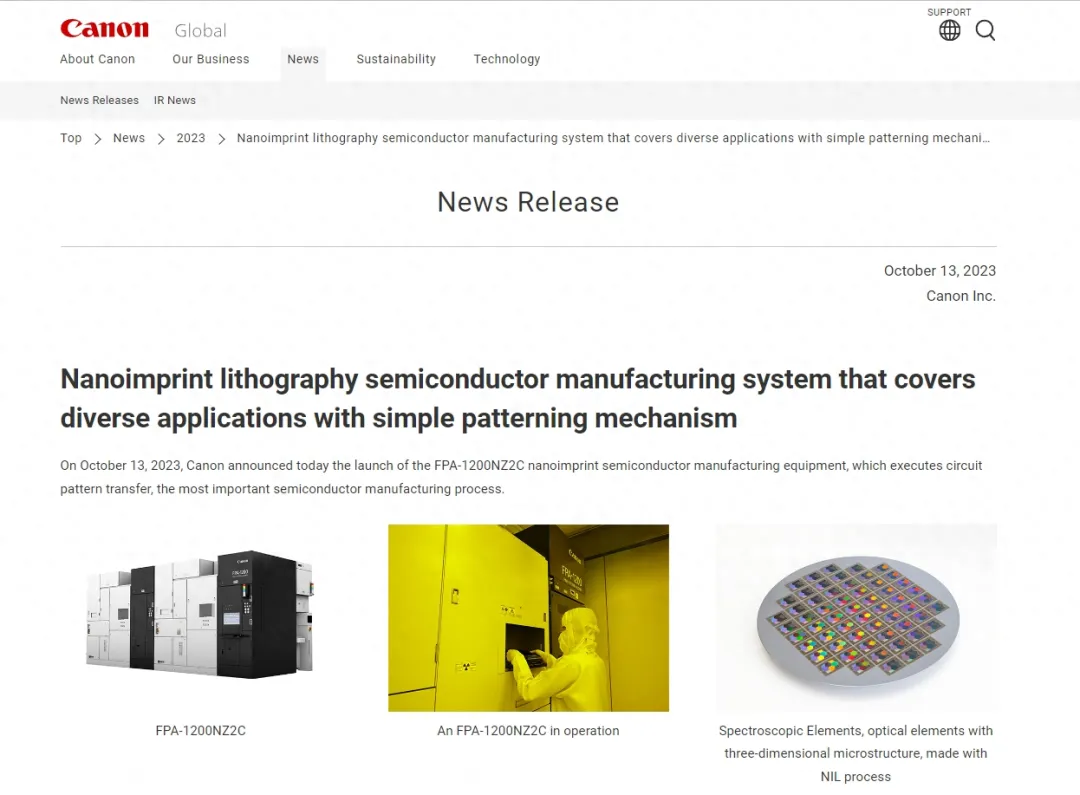
The world of technology and innovation is ever-evolving, and one such stride that has taken the semiconductor industry by storm is Canon’s latest groundbreaking achievement. On October 13th, Canon’s official website proudly announced the launch of their newest Nanoimprint Lithography (NIL) device, the FPA-1200NZ2C. This advanced piece of technology promises to revolutionize the semiconductor manufacturing landscape, pushing the boundaries of what was previously thought possible.
01
A Glimpse into the Future of Nanoimprint Lithography
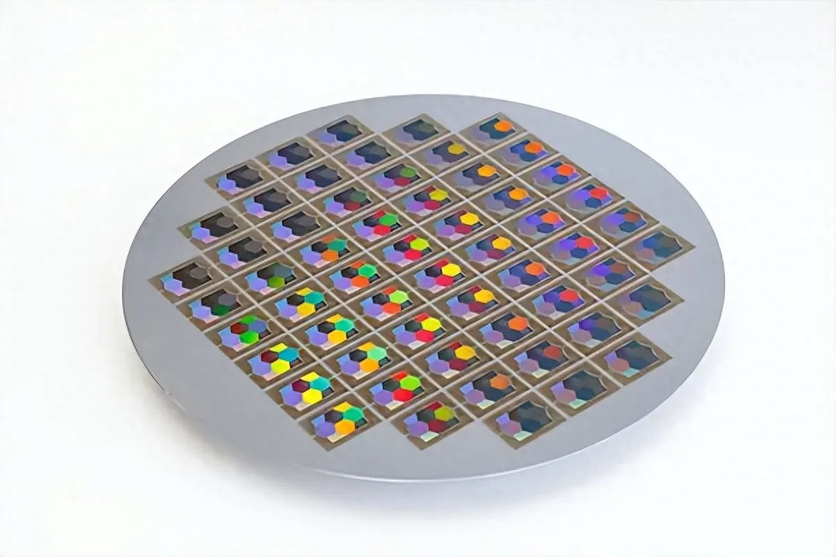
Nanoimprint Lithography, or NIL, is a cutting-edge manufacturing technology that allows for the creation of intricate circuit patterns directly onto silicon wafers. Unlike traditional photolithography methods that require exposing circuit patterns onto silicon wafers, NIL is akin to using a stamp to imprint these patterns. This process not only streamlines production but also results in significant energy savings and cost reductions, all thanks to its straightforward equipment structure.
02
Breaking Down the Technical Marvel
What truly sets the FPA-1200NZ2C apart from its predecessors is its capability to achieve patterned features as small as 14nm. To put this into perspective, these dimensions are equivalent to the production of the most advanced 5nm logic chips currently available in the market. Furthermore, Canon’s commitment to innovation aims to push the envelope even further, with expectations of achieving a minimum line width of 10nm for circuit patterns, equivalent to astonishing 2nm logic nodes.
This outstanding technological achievement demonstrates Canon’s unwavering dedication to pioneering cutting-edge solutions for the semiconductor industry.

03
Navigating Export Controls
In light of the Japanese government’s decision to include advanced process equipment in export controls, questions have arisen about whether NIL devices fall under this purview. Canon, in response, has assured stakeholders that they are fully committed to complying with all regulatory standards. This commitment ensures the technology’s accessibility while maintaining transparency and adhering to international trade guidelines.
04
Challenging the Status Quo
One of the most intriguing aspects of this development is Canon’s bold challenge to the Dutch company ASML, which has, for some time, held a near-monopoly on advanced photolithography technology. Canon, traditionally ranked third in the global photolithography equipment market, is making a power move with its NIL devices. This bold step not only shakes up the industry’s hierarchy but also signifies Canon’s unwavering commitment to innovation and technological advancement.
05
A Legacy of Innovation
The journey towards this groundbreaking technology has been marked by dedication and perseverance. In 1995, Chinese-American scientist Professor Stephen Chou introduced the concept of nanoimprint, setting the stage for research into nanoimprint manufacturing technology. In 2009, the U.S.-based company Molecular Imprints (MII) embarked on a journey to utilize NIL technology for 32nm logic node production. Despite initial promise, mass production proved elusive, primarily due to efficiency, defect rates, and financial issues.
Fast forward to 2014, and Canon entered the NIL market by acquiring MII. This move was far from impulsive, as Canon had been secretly developing nanoimprint technology since 2004, only revealing it to the world post-acquisition. Collaborating with Japanese photomask manufacturer Dai Nippon Printing and KLA (formerly Toshiba), Canon has been diligently working on enhancing NIL technology. They even ventured into memory storage manufacturing with KLA and SK Hynix, thereby showcasing their commitment to innovation and pushing the boundaries of semiconductor manufacturing.
06
The Challenges of NIL Technology
While the advantages of NIL technology are evident, its journey to becoming mainstream is fraught with challenges. The precision and frequency of contact required in the NIL process result in wear and tear of both the mask and silicon wafer surfaces. Additionally, issues related to their lifespan, stress, and accuracy pose formidable hurdles. While NIL devices may avoid the precise optical path requirements of other lithography methods, they still need to overcome a series of material science and mechanical issues to match the production capabilities of EUV lithography machines.
These challenges are a stark reminder of the uphill battle that Canon has chosen to undertake, as they pave the way for the future of semiconductor manufacturing.
07
A Promising “Backup” in Semiconductor Manufacturing
NIL technology stands as a promising “backup” in the semiconductor manufacturing landscape. Its advantages are undeniable, with the potential to revolutionize the industry by streamlining production and reducing costs. However, these same advantages also highlight why NIL technology has not yet been adopted for mass production by any major company.
The journey from technological breakthrough to commercialization is a challenging one, filled with obstacles that can often feel insurmountable. Canon’s unwavering commitment to overcoming these challenges and reshaping the industry is a testament to their dedication and the transformative potential of NIL technology.
08
In Conclusion
Canon’s unveiling of the FPA-1200NZ2C Nanoimprint Lithography device marks a significant milestone in the world of semiconductor manufacturing. With the capability to produce intricate circuit patterns at unprecedented nanoscale dimensions, Canon is setting a new standard for the industry. Their determination to challenge the established order and the bold steps taken in the face of technical challenges demonstrate their commitment to innovation.
As the industry eagerly anticipates the future of NIL technology, Canon’s legacy of innovation and its resolve to overcome obstacles stand as a beacon of hope for the semiconductor manufacturing landscape.


