
Memory technology, as a core component of computer systems, plays a crucial role in enhancing overall computing capabilities. Against this backdrop, High Bandwidth Memory (HBM) is gradually emerging in the field of memory technology with its outstanding performance, becoming a key force in driving the computing field into a new era.
01
Far Beyond DDR: The Next Revolution in Memory Technology
DDR is a common type of computer memory that was originally designed to improve memory transfer rates. It employs double data rate technology, allowing for two data transfers per clock cycle, thus enhancing the data transfer rate.
The most common versions of DDR today are DDR4 and DDR5, but in the past, there were also DDR3, DDR2, and DDR versions. Each generation of DDR has different data transfer rates and performance.
DDR memory is typically used as system memory in computers, storing data for the operating system and applications that are currently running.
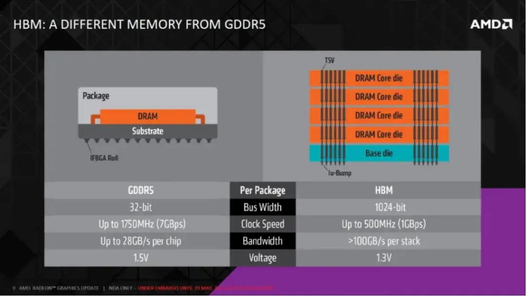
HBM is a high-bandwidth memory technology focused on providing higher memory bandwidth, especially suitable for high-performance computing and graphics processing areas. A significant feature of HBM is its use of stacking technology, vertically stacking multiple DRAM chips, thereby greatly increasing the data path and improving memory bandwidth.
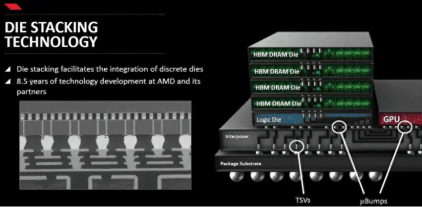
Therefore, HBM has the characteristic of being scalable to larger capacities. Not only can the capacity of HBM’s single DRAM chip layer be expanded, but HBM can also achieve greater memory capacity through methods such as stacking 4, 8, or even 12 layers of DRAM chips, as well as integrating multiple HBM stacked DRAM chips through SiP (System in Package).
HBM memory is commonly used in high-performance graphics cards, GPU accelerators, and high-performance computing applications that require a large amount of data transfer.
From a power consumption perspective, due to the use of TSV (Through-Silicon Vias) and micro-bump technology, a shorter signal transmission path and lower per-pin I/O speed and I/O voltage between the DRAM bare die and the processor are achieved, giving HBM better memory power efficiency characteristics. Based on the normalized per-pin I/O bandwidth power consumption ratio of DDR3 memory, the I/O power consumption ratio of HBM2 is significantly lower than that of DDR3, DDR4, and GDDR5 memory, with a 42% reduction in the per-pin I/O bandwidth power consumption ratio compared to GDDR5 memory.
In terms of system integration, HBM integrates all DDR memory chips and CPU chips on the PCB into the SiP, thus HBM also has advantages in saving product space. Compared to GDDR5 memory, HBM2 saves 94% of chip area.
02
Inside the Innovation Journey: The Development Sagas of the Top Three Manufacturers
The current HBM market is mainly dominated by three companies: SK Hynix, Samsung, and Micron.
In 2014, SK Hynix and AMD jointly developed the world’s first silicon through-hole HBM, and to date, they have iterated and upgraded 4 generations of HBM products, continuously improving performance and capacity. In 2020, SK Hynix announced the successful development of the new generation HBM2E; in 2021, they developed the world’s first HBM3; in 2022, HBM3 chips were supplied to Nvidia. In August 2023, SK Hynix launched the HBM3E, and in November, Nvidia announced that the H200 would be equipped with the HBM3E.
From HBM1, HBM2E, and HBM3, to HBM3E, SK Hynix has continuously led the way. In 2022, SK Hynix held about 50% of the HBM market share, Samsung 40%, and Micron 10%.
For a long time, SK Hynix was the exclusive supplier of HBM for Nvidia. In 2023, SK Hynix almost monopolized the supply of HBM3, and this year, its orders for HBM3 and HBM3E are already sold out.
Samsung announced the mass production of 4GB/8GB HBM2 DRAM in 2016; in 2018, they announced the mass production of the second generation 8GB HBM2; in 2020, they launched the 16GB HBM2E product; in 2021, Samsung developed HBM-PIM with AI processing capabilities. Although Samsung’s roadmap showed that HBM3 technology was in mass production in 2022, Samsung’s HBM3 was only officially verified at the end of 2023, meaning the market was still monopolized by SK Hynix before mass production.
Looking at Micron, in 2020, Micron announced it would start providing HBM2 memory/VRAM; in 2021, HBM2E products were launched. To improve its passive position in the HBM market, Micron chose to skip the fourth generation of HBM, namely HBM3, and directly upgrade to the fifth generation, HBM3E. Subsequently, in September 2023, Micron announced the launch of HBM3 Gen2 (i.e., HBM3E) and later stated plans to start mass shipments of HBM3 Gen2 memory in early 2024, revealing that Nvidia is one of its main customers.
03
From HBM2e to HBM3e: The Evolutionary Leap in Memory Tech Unveiled
The rise of the concept of HBM (High Bandwidth Memory) is directly related to the boom in AI-generated content (AIGC).
The emergence of large AI models has led to a massive demand for computational power, and the significant increase in data processing and transfer rates has made AI servers demand higher chip memory capacity and bandwidth. HBM, with its advantages of high bandwidth, high capacity, low latency, and low power consumption, has gradually become the standard for GPUs in AI servers.
Currently, HBM products have been developed in the order of HBM (first generation), HBM2 (second generation), HBM2E (third generation), HBM3 (fourth generation), and HBM3E (fifth generation), with the latest HBM3E being an expanded version of HBM3.
| Category | HBM1 | HBM2 | HBM2E | HBM3 | HBM3E |
|---|---|---|---|---|---|
| BW (GB/s) | 128 | 307 | 460 | 819 | 1000 |
| Stack Height (Layer) | 4 | 4/8 | 4/8 | 8/12 | 8/12 |
| Capacity (GB) | 1 | 4/8 | 8/16 | 16/24 | 24/36 |
| I/O (Gbps) | 1 | 2.4 | 3.6 | 6.4 | 8.0 |
| JEDEC Release Date | Jan. 2016 | Dec. 2018 | Feb. 2020 | Jan. 2022 | Aug. 2023 |
| Channels | 8 | 8 | 12 | 16 | 16 |
| Storage number per channel | 128MB | 1GB | 1GB | 1.5GB | TBD |
| Process node | 29nm | 21nm | 10nm | 5nm | 10nm |
| Effective bit width | 1024-bit | 1024-bit | 1024-bit | 1024-bit | 1024-bit |
| Voltage | 1.2 | 1.2 | 1.2 | 1.1 | TBD |
| Transfer Speed | 1GT/sec/pin | 2GT/sec/pin | 3.2GT/sec/pin 3.65GT/sec/pin | 6.4GT/sec/pin 6.4GT/s | 8GT/s |
| Total channel width | 1024 bits (8-Hi stack) | 1024 bits (8-Hi stack) | 1024 bits (8-Hi stack) | 1024 bits (8-Hi stack) | 1024 bits (8-Hi stack) |
Each update and iteration of HBM is accompanied by an increase in processing speed. The pin data transfer rate of the first-generation HBM was 1Gbps, which has developed to 8Gbps in the fifth-generation product HBM3E, meaning it can process 1.225TB of data per second. In other words, downloading a 163-minute full HD movie (1TB) would take less than a second.
Of course, the capacity of the memory is also continuously increasing. The maximum capacity of HBM2E is 16GB. Currently, Samsung is using EUV lithography machines to manufacture HBM3 chips with a capacity of 24GB. Moreover, stacking 8 or 12 layers can achieve a capacity of 36GB (the industry’s largest) on HBM3E, which is 50% higher than HBM3.
SK Hynix and Micron have both announced the launch of HBM3E chips, each capable of achieving more than 1TB/s of bandwidth.
According to a survey by TrendForce, the mainstream market for HBM in 2023 is HBM2e, including NVIDIA A100/A800, AMD MI200, and most self-developed accelerator chips by CSPs designed with this specification. Meanwhile, to meet the evolving demands of AI accelerator chips, manufacturers plan to launch new products, HBM3e, in 2024, with HBM3 and HBM3e expected to become the mainstream in the market next year.
04
HBM3e Ignites the Market: Unleashing the Next Wave of Memory Revolution
SK Hynix is undoubtedly the biggest beneficiary of this memory boom, with significant revenue growth in the fiscal year 2023 and the fourth quarter up to December 31, 2023. Especially its main products, DDR5 DRAM and HBM3, saw a revenue increase of more than four times compared to the previous year.
Nvidia and AMD’s next-generation artificial intelligence GPUs are expected to mainly use HBM3 memory. For example, the H100 is the first GPU to support the PCIe 5.0 standard and the first to use HBM3, supporting up to six HBM3 chips with a bandwidth of 3TB/s, which is 1.5 times that of the A100 using HBM2E, with a default memory capacity of 80GB.
In November 2023, Nvidia released a new generation of AI GPU chips, H200, and AI server platform products such as HGX H200. This GPU is an upgrade of the H100, still using the Hopper architecture and TSMC’s 4nm process. According to Nvidia’s official website, the H200’s GPU chip has not been upgraded, with no change in core count or frequency. The main upgrade is the first use of HBM3e memory, and the capacity has been increased from 80GB to 141 GB.
Thanks to the newly upgraded HBM3e chip, the H200’s memory bandwidth can reach 4.8TB/s, a 43% increase over the H100’s 3.35TB/s. However, this is far from reaching the upper limit of HBM3e. Analysts abroad claim that Nvidia intentionally reduced the speed of HBM3e to pursue stability. Compared to traditional x86 servers, the H200’s memory performance can be up to 110 times higher.
Since the HBM3e chips from Micron, SK Hynix, and other companies will not be shipped until 2024, Nvidia stated that the H200 products are expected to officially go on sale in the second quarter of 2024.
AMD’s MI300 also uses HBM3, with the MI300A having the same capacity as the previous generation at 128GB, and the higher-end MI300X reaching 192GB, a 50% increase. AMD claims that the MI300X offers the highest HBM density, 2.4 times that of Nvidia’s AI chip H100, and its HBM bandwidth is 1.6 times that of the H100. This means AMD’s chips can run larger models than Nvidia’s chips.
Meanwhile, in 2023, with the surge in AI GPUs and related demands, HBM prices have continued to rise. A report by market research firm Yolo Group shows that during 2023, there was a significant change in the HBM memory supply chain, with production levels and adoption rates increasing significantly, making HBM a more valuable resource than before the AI boom. The average selling price of HBM chips in 2023 was five times that of traditional DRAM memory chips.
In the current era of HBM prevalence, no memory manufacturer can resist sharing in the benefits.
05
The Big Three Go Wild: The Frenzy Behind the Latest Memory Tech Breakthrough
Technology upgrade
At SEMICON Korea 2024, SK Hynix made an important announcement, unveiling its ambitious high-bandwidth memory roadmap. The company’s vice president, Kim Chun-hwan, revealed plans to begin mass production of the advanced HBM3E in the first half of 2024, emphasizing the delivery of 8-layer stacked samples to customers.
HBM3E, the latest product in SK Hynix’s lineup, is designed to meet the growing data bandwidth demands, offering 1.2 TB/s per stack and an astonishing 7.2 TB/s communication bandwidth in a 6-stack configuration. Kim Chun-hwan attributed the urgency of this advancement to the rapid rise of generative artificial intelligence, expecting to witness an impressive 35% compound annual growth rate (CAGR). However, he warned that the semiconductor industry is facing “fierce survival competition” driven by continuously escalating customer expectations.
As the semiconductor industry’s process technology nodes shrink and approach their limits, there is an increasing focus on next-generation memory architectures and processes to unlock higher performance. SK Hynix has already initiated the development of HBM4, planning to offer samples in 2025 and start mass production the following year.
According to Micron, compared to previous generations of HBM, HBM4 will utilize a wider 2048-bit interface, leading to a theoretical peak memory bandwidth of over 1.5 TB/s per stack. To achieve these extraordinary bandwidths while maintaining reasonable power consumption, HBM4 aims for a data transfer rate of about 6GT/s. This wider interface and faster speed will enable HBM4 to break through memory bandwidth limits, meeting the growing demands of high-performance computing and AI workloads.
Samsung, a major player in the semiconductor industry, also has a timeline for HBM4, planning to provide samples in 2025 and start mass production in 2026. Samsung executive Jaejune Kim revealed that over half of the company’s HBM production is already composed of specialized products. The trend toward customized HBM solutions is expected to intensify. Tailored options, through logic integration, are crucial for meeting personalized customer demands, thus solidifying market position.
With the release of HBM3E and the preparation for HBM4, SK Hynix and Samsung are gearing up for future challenges, aiming to maintain their leading positions in HBM technology. Furthermore, the top three global memory chip manufacturers are shifting more capacity to HBM production, but as capacity adjustments take time, it is difficult to rapidly increase HBM output, and the HBM supply is expected to remain tight for the next two years.
Expansion Situation
Regarding the expansion plans of the three major manufacturers, it’s reported that SK Hynix will increase its investment in high-bandwidth memory production facilities to meet the rising demand for high-performance AI products.
In June last year, media reports stated that SK Hynix was preparing to invest in backend process equipment and expand its Cheongju plant for packaging HBM3. It’s expected that by the end of this year, the scale of the plant’s backend process equipment will nearly double.
Additionally, SK Hynix plans to build one of the most advanced manufacturing plants in Indiana, USA. According to two sources interviewed by the Financial Times, SK Hynix will produce HBM stacks at this factory, which will be used in Nvidia GPUs manufactured by TSMC. The SK Group chairman stated that the factory is expected to cost $22 billion.
The competition between Samsung Electronics and SK Hynix is heating up. Samsung Electronics started to expand the supply of the fourth generation HBM, HBM3, in the fourth quarter of last year and is currently in a transition period. In January this year, Han Jin-man, Executive Vice President of Samsung’s semiconductor business in the US, said the company has high hopes for its high-capacity storage chips, including the HBM series, hoping it will lead the rapidly growing field of artificial intelligence chips. At CES 2024’s media briefing, he told reporters, “Our HBM chip production this year will increase by 2.5 times compared to last year, and will double again next year.”
Samsung also revealed plans to increase HBM’s maximum output to 150,000 to 170,000 units per month before the fourth quarter of this year, aiming to compete in the HBM market in 2024. Previously, Samsung Electronics spent 10.5 billion Korean won to acquire a factory and equipment in Cheonan, South Korea, from Samsung Display to expand HBM capacity. It also plans to invest between 700 billion to 1 trillion Korean won in building new packaging lines.
To close the gap, Micron is betting big on its next-generation product, HBM3E. CEO Sanjay Mehrotra stated, “We are in the final stages of validation for providing HBM3E for Nvidia’s next-generation AI accelerators.” The company plans to start mass shipping HBM3E memory at the beginning of 2024, emphasizing that its new product has attracted significant interest across the industry. It’s reported that Micron Technology’s Taichung Plant 4 in Taiwan, China, was officially operational in early November 2023. Micron stated that Taichung Plant 4 would integrate advanced detection and packaging testing functions to mass-produce HBM3E and other products, thereby meeting the growing needs of various applications such as artificial intelligence, data centers, edge computing, and cloud. The company plans to start mass shipments of HBM3E in early 2024.
It’s worth noting that the competition for advanced HBM is just beginning. Although the current HBM products still account for a very small portion of overall storage shipments, in the long term, as consumer electronics evolve towards AI, the main demands will be for high computing power, high storage, and low energy consumption. Given this, it’s expected that HBM will also become a future technological development direction for storage manufacturers.

Related:
- HBM4 Memory Standard: Boosts Bandwidth and Efficiency
- PCIe 6.0 SSD from SK hynix Coming Soon with HBM3E
- SK Hynix Strategic Approach to Maintaining Competitiveness
- Revolution of High Bandwidth Memory (HBM) in the Age of AI
- New 24GB HBM3E by Micron: Powering NVIDIA’s H200!
- Storage Chips Clash Again: Opportunities Await You!
- Samsung Leverages SK Hynix Tech for Chip Manufacturing!
- Revolutionizing HBM4: Samsung 16 Layers Stacking Success!
- TSMC CoWoS Capacity Skyrockets by 150% Due to NVIDIA!
- TrendForce: HBM Prices to Climb 5-10%, Over 30% of DRAM
- DDR3 Costs Rising as Manufacturers Stop Supply in late 2024

Disclaimer: This article is created by the original author. The content of the article represents their personal opinions. Our reposting is for sharing and discussion purposes only and does not imply our endorsement or agreement. If you have any objections, please get in touch with us through the provided channels.


