Guide: Recently, according to a report by Nikkei News, TSMC founder Morris Chang said that AI clients have contacted him, hoping to build ten new wafer fabs for artificial intelligence processors.

TSMC founder Morris Chang stated at the completion ceremony of its Japanese subsidiary (JASM), “They are not talking about tens of thousands of wafers, but about wafer fabs, ‘We need so many wafer fabs, possibly three, five, or ten wafer fabs.’ Well, I can hardly believe it.”
Chang mentioned that the demand for AI processors might fall in between, “somewhere between tens of thousands of wafers and several dozen wafer fabs.“
Tom’s Hardware reported that this demand is not surprising, as the demand for AI processors has surged, and major GPU manufacturer Nvidia has been unable to meet the chip supply. Companies like OpenAI also lack sufficient AI computing power.

Since the beginning of the year, OpenAI’s CEO has stated that they are seeking capital to support a $7 trillion AI chip manufacturing plant. Jensen Huang commented that this amount of money would be enough to buy all the GPUs, while the total value of all global data centers is only $1 trillion.
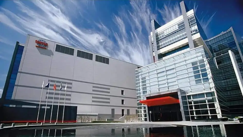
TSMC is one of the few semiconductor manufacturers globally that has a wafer production capacity of about 100,000 pieces per month. To operate a mega wafer fab (referred to by TSMC as GigaFab), TSMC needs to reuse expensive equipment across different processes, maximizing production capacity utilization and cost optimization.
However, the cost of building a large, advanced wafer fab is very high. A 3nm process wafer fab, fully built and equipped with all machines, could cost over $20 billion and take several years to construct. Financial reports show that TSMC’s capital expenditures for 2024 are between $28 billion and $32 billion, so they won’t build multiple GigaFabs every year.
In theory, the cost of ten new advanced wafer fabs would exceed $200 billion, and at the current construction pace, it would take over 20 years to complete and start production. This does not include supply chain support and infrastructure costs, making it unfeasible for TSMC to bear this expense.
At the same time, although the trillion-dollar investment plan in AI chip wafer fabs is vast, it is nearly impractical in business terms. High-end AI, HPC, and smartphone SoCs all require advanced processes with a production cycle of about 2-3 years before moving on to more advanced processes. Building 10 wafer fabs simultaneously would not only risk severe overcapacity but could also lead to massive losses or even bankruptcy for the foundries due to the depreciation of expensive equipment.
Currently, TSMC operates 6 12-inch mega wafer fabs, 6 8-inch wafer fabs, and 1 6-inch fab. The construction and upgrade of these fabs span two centuries and over 30 years, experiencing several cycles of shortage and surplus. For example, the recently operational Japanese fab JASM was established with substantial subsidies, visible stable orders, and joint funding from major customers like Sony, Denso, and Toyota.
Related:

Disclaimer: This article was created by the original author from Taiwan Strait Network. The content of the article represents their personal opinions. Our reposting is for sharing and discussion purposes only and does not imply our endorsement or agreement. If you have any objections, please contact us through the provided channels.


