
Although systems based on intermediary layers can be created today, the tools and methodologies are not yet perfected and there are mismatches with organizations.
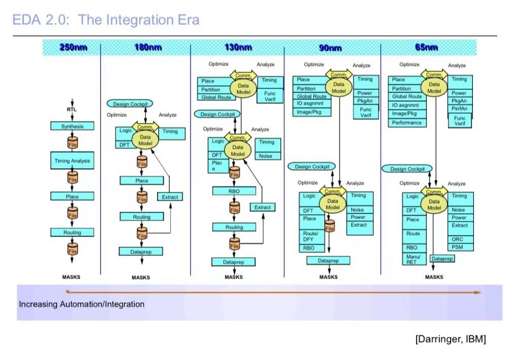
Flaws in the EDA toolchain for 2.5D design limit the application of this advanced packaging method, which is currently mainly confined to the high-performance computing domain. However, as other parts of the semiconductor industry begin to advance toward higher-level packaging and chiplet technologies, the EDA industry is starting to adjust its development direction.
All new technologies have a learning period, and 2.5D advanced packaging technology is no exception. Although the potential of this packaging method is clear—offering more functionality, lower power consumption, and higher performance than an SoC of retinal size—the EDA industry is quite cautious about this market. Until recently, it was unclear which of the numerous packaging schemes would gain enough market share to justify investment. However, with financial markets forecasting a larger application scale for high-bandwidth memory (HBM) and progress in 2.5D technology leading to the first proof of concept, the market situation has started to change positively.
To achieve widespread adoption of 2.5D technology, much optimization and automation work is still needed, and it remains to be seen which of the various potential solutions will prevail. However, as standards are gradually introduced and the industry continues to advance this packaging technology, the related tools need to become more efficient and elegant in addressing a range of challenges.
01
Interface
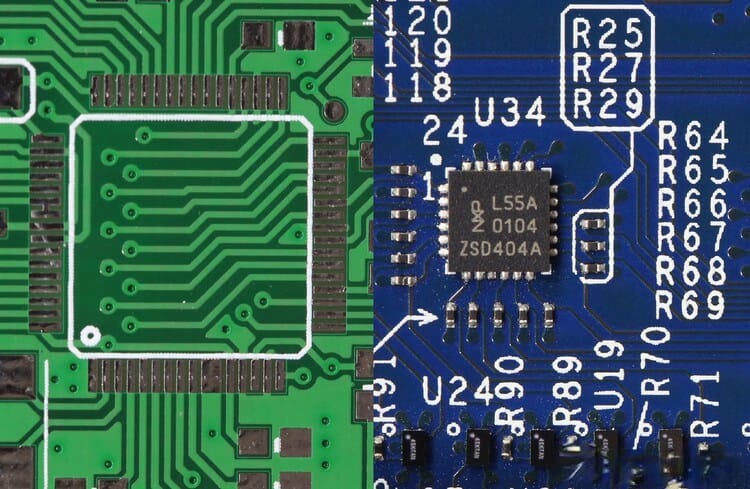
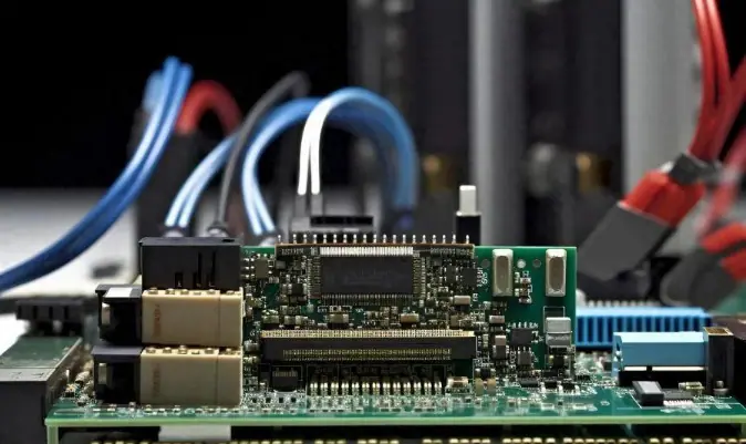
The introduction of a new type of connection, which was not present before, is one of the biggest challenges but also an opportunity in 2.5D integration. Although previous designs had the same on-chip connections, 2.5D uses an intermediary for connection. From this perspective, they resemble PCBs (printed circuit boards) but with a connection density closer to that of the most advanced planar chips.
John Park, head of the Cadence Custom IC & PCB Group’s product management team, said, “When you start making independent chip components and inserting PHY for UCIe, you face the classic problem of signal integrity. Is it compliant when a UCIe interface on this chip component is connected to another UCIe interface through an intermediary layer or bridge? How big is the jitter? Is there too much noise on the line causing my receiver eye to shrink? The processing done on the chip design side and the system side is gradually converging. The system side has over 30 years of experience dealing with signal integrity and we have advanced three-dimensional electromagnetic field solvers that allow you to model it. For digital chip designers, this concept might be somewhat novel.”
Now, the tools used by integrated circuit designers are more like circuit board tools, but over time, this will become more like a chip-level issue. Marc Swinnen, director of product marketing at Ansys, said, “Current communication is still very similar to PCBs, it is coarse-grained. The industry is moving toward finer granularity, we see chiplet connections move from C4 bumps to micro-bumps, then to hybrid bonding, and the interconnect density is getting higher. With finer granularity and 3D architecture, you can consider the communication of functional modules with other modules. Theoretically, it could evolve much further, but designing and laying out with existing tools is just too difficult.”
There is a learning cycle involved, concerning socket materials and design as well as related communication standards. Ramin Farjadrad, CEO and co-founder of Eliyan, said, “UCIe has two versions, one for advanced packaging and one for standard packaging. For advanced packaging, the wire distance is 2 millimeters; but for standard packaging, it’s 20 to 25 millimeters. If you want to achieve the highest bandwidth, using standard packaging is much more difficult than using advanced packaging. In advanced packaging, you can reach 32Gbps using basic SerDes. You don’t worry about crosstalk or channel return loss. Because the wire density is very high, you can place high-speed wires within the wire shield, without additional vias. But in standard packaging, you must use vias, which causes crosstalk and reflection.”
Despite everything seemingly favoring advanced packaging, the reality is not that simple. Farjadrad added, “While the line density may be 5 to 6 times lower than that of advanced substrates, this means the line cross-sectional thickness can be increased by 5 to 6 times. This results in a 30-fold reduction in resistance for the same wires, allowing for longer distance transmission. This is a compromise between high speed and low resistance.”
Advanced packaging in UCIe relies on its very short transmission distances. Tony Mastroianni, director of Advanced Packaging Solutions at Siemens Digital Industries Software, said, “Therefore, you don’t need to use many of the advanced equalization techniques found in long-distance SerDes. This results in them being smaller in size, lower in power consumption. They are ideal transmitters and receivers, hence avoiding the distortion issues that can arise in packaging channels. You do need to carefully lay out these traces and deal with spacing and shielding issues to ensure performance isn’t lost due to less-than-ideal wiring between chips. Most existing PHY designs leverage their short-distance nature. This creates a problem because you can only place a limited amount of HBM memory on a chip. You can’t place them too far from a small chip because these PHYs are not designed for that.”
Other tools need significant upgrades. Andy Heinig, head of the Efficient Electronics department at Fraunhofer IIS/EAS, said, “3D systems contain massive power delivery networks in different parts of the system. There’s a grid on the chip, copper pillars or hybrid bonding pads between chips, and other elements outside the system—usually the package substrate. The entire power network is a very complex structure, containing millions of design elements of varying sizes. Design elements on the chip are within tens of microns, while structures on the package can be up to several millimeters. For 3D solvers, this kind of multi-level problem is usually difficult to solve, but it’s still necessary to simulate the entire power grid to verify the power network.”
Power issues are more like integrated circuit tools than printed circuit board tools. Siemens Digital Industries Software’s Mastroianni said, “Power is typically supplied from the bottom-layer transistors and passed upwards, although the related tools can provide assistance, they still need to be managed. In 3D designs, the entire device will use millions or tens of millions of hybrid bonds to fill. Compared to traditional chip designs where power and ground networks are pre-designed, you just need to configure a uniform grid across the entire chip to manage power. The layout and routing tools will determine which contacts are used for power transmission.”
02
Variability Issues
As systems evolve towards 2.5D and 3D, on-chip variation (OCV) issues become more pronounced. Mastroianni stated, “Timing closure and OCV become enormous challenges. Since there is no longer reliance on a single wafer, process variations will be greatly exacerbated. If microchip modules are manufactured using different processes, they will lose correlation. For a single transistor, you rely on its internal correlation; however, when using different technologies, suppliers, and wafers, this correlation disappears.”
Not just process changes need attention, but temperature variations as well. Ansys’ Swinnen said, “Temperature fluctuations can lead to significant device behavior changes beyond the static timing analysis minimum/maximum temperature range. Mechanical stress has a significant impact on the electrical parameters of semiconductor devices. In fact, many processes intentionally introduce mechanical stress during transistor manufacturing to influence their characteristics. Solutions to translate mechanical results into electrical impacts are still being developed. Additionally, some are looking at integrating photonics into the packaging, but photonic circuits are very temperature-sensitive, even small changes can cause parameter failures.”
Corner issues could affect each other. Cadence’s Park said, “To solve timing issues, you have to consider multiple aspects, like process, power, and thermal management. As these issues accumulate, the complexity of the problem increases. How do we solve it? We already have some techniques to weaken corner issues. When we apply 3D stacking and hybrid bonding, the industry wants to see similar processes, close nodes, and similar timing performance to make the solution more manageable.”
In the past, we dealt with variability issues by adding margins. Mastroianni stated, “If you try to solve all the process variability and performance issues, excessive margins will make the design exceedingly complex. Therefore, we need to set interfaces between modules to fundamentally achieve high-speed synchronization. This can decouple these variations and achieve a highly synchronized high-speed interface between two modules.”
03
EDA Tool Development
The EDA industry is striving to solve these and other issues. Kent Stahn, senior manager of hardware engineering in the Solutions Group at Synopsys, said, “In this field, some packaging-centric tools are trying to address all the issues. Meanwhile, some tools originating from the silicon field are evolving to face the future, such as RDL fan-out packaging, etc. From a layout perspective, these tools are making constant progress. Next is the analysis part, we see the integration between analysis tools and layout tools becoming increasingly excellent.”
However, there’s still a lot of work to be done. Park stated, “Currently, the vast majority of tools are extensions of packaging design tools. Over 75% of interposers are made with tools modified over the past decades in the printed circuit board and laminate packaging fields. These tools have been adjusted for power. We needed a different power router, so we added that function. However, when I’m doing laminate packaging, there’s no formal DRC or LVS. They run some CAM tools, ensuring there are no spacing violations and sharp corners, but this approach is quite informal. We don’t manufacture chips this way. We use very formal DRC and LVS processes to ensure the output is clean and manufacturable.”
The signoff process has been deeply integrated into the chip development methodology. Swinnen asked, “Why do people rely so much on the signoff phase? When 3-nanometer technology came out, no one had a lot of experience, the same goes for 3D interconnectors. Everyone acknowledges that the actual application of solvers is still not very common. You need a solver that has shown in the past that it can handle unexpected situations well, with good adaptability, broad application, and enough precision. This is also why people are so conservative in the signoff phase and reluctant to change. They want the solver to be able to handle various issues correctly and reliably.

One of the key upgrade needs is to analyze factors beyond resistance R and capacitance C. Synopsys’ Stahn stated, “Chip designers often ignore inductance L, and it is actually very important. That’s why package designers, chip designers, and printed circuit board designers need to come together, multiple disciplines collaborating. There are different tools to choose from, for instance, tools that can be integrated into layout tools or standalone tools for signal integrity analysis. As long as chip designers start paying attention to inductance L and change their way of thinking, this is entirely feasible. For traditional silicon extraction tools, they also need to start paying attention to this. Because as the size of the interconnect increases, circuit lengths get longer, speeds go up, they are getting closer and closer to a wavelength or a tenth of a wavelength. We have to consider this, otherwise, we’ll face signal integrity issues.”
Compared to the past, architects need more help. “Everyone needs a system planner,” Park said, “You’re not just designing a single chip, but three integrated chips. From a higher level, you need a system planner to integrate these chip components, optimize their placement, focus on thermal design and power transmission, and create an optimized 3D blueprint based on this. Then you can use one tool to design the digital chip components, another tool to design the analog chip components, and finally do the packaging. From a tool perspective, system-level planning has made great progress, but we’re just expanding their databases and adding new features.”
The biggest change might be at the organizational level. Mastroianni stated, “In the past, package designers never communicated with architects. But now they must. Which implementation technology will be chosen? How will thermal issues be handled? Which packaging technology will be used? Is it a silicon interposer or an organic interposer? Because there are infinitely many scenarios, analysis needs to be done as early as possible. How to decompose the system or subsystem into many chiplets? At the architectural decomposition level, you at least need to consider stress analysis. When starting physical design, package designers need to work with chip designers on I/O planning. In addition, testing methods need to be considered, test engineers need to collaborate with packaging engineers to discuss which testing strategies to use in the chiplet set, and how to connect them in the package.”
04
Conclusion
EDA companies have already made improvements to existing tools to implement and verify 2.5D systems. However, these tools may not be sufficient to make 2.5D integration mainstream, as the tool and design team structures may not fully align. Although the optimal organizational structure is still up for debate, ultimately they need to work together and collaborate. Problems often hide in the details, and based on today’s methodologies, there are many pitfalls and unknowns, leading to potential disasters waiting to happen.

Disclaimer: This article is created by the original author. The content of the article represents their personal opinions. Our reposting is for sharing and discussion purposes only and does not imply our endorsement or agreement. If you have any objections, please contact us through the provided channels.


