
| Category | HBM1 | HBM2 | HBM2E | HBM3 | HBM3E |
|---|---|---|---|---|---|
| BW (GB/s) | 128 | 307 | 460 | 819 | 1000 |
| Stack Height (Layer) | 4 | 4/8 | 4/8 | 8/12 | 8/12 |
| Capacity (GB) | 1 | 4/8 | 8/16 | 16/24 | 24/36 |
| I/O (Gbps) | 1 | 2.4 | 3.6 | 6.4 | 8.0 |
| JEDEC Release Date | Jan. 2016 | Dec. 2018 | Feb. 2020 | Jan. 2022 | Aug. 2023 |
| Channels | 8 | 8 | 12 | 16 | 16 |
| Storage number per channel | 128MB | 1GB | 1GB | 1.5GB | TBD |
| Process node | 29nm | 21nm | 10nm | 5nm | 10nm |
| Effective bit width | 1024-bit | 1024-bit | 1024-bit | 1024-bit | 1024-bit |
| Voltage | 1.2 | 1.2 | 1.2 | 1.1 | TBD |
| Transfer Speed | 1GT/sec/pin | 2GT/sec/pin | 3.2GT/sec/pin 3.65GT/sec/pin | 6.4GT/sec/pin 6.4GT/s | 8GT/s |
| Total channel width | 1024 bits (8-Hi stack) | 1024 bits (8-Hi stack) | 1024 bits (8-Hi stack) | 1024 bits (8-Hi stack) | 1024 bits (8-Hi stack) |
The race to develop “Wideband Memory (HBM)” is heating up. Companies like Samsung Electronics are turning to SK Hynix, a leader in semiconductor stack technology, to increase their data processing capabilities. The popularity of HBM represents a great business opportunity for Japanese tools and equipment supporting high-tech technologies.
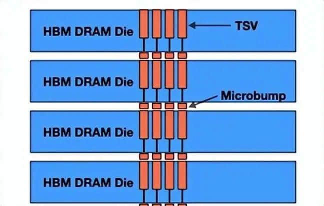
HBM is a new type of semiconductor device that stores multiple DRAM chips to increase data processing capacity. Demand is increasing exponentially with the rise of artificial intelligence (AI), which requires rapid processing of large amounts of data.
As the miniaturization of semiconductor circuits approaches its visible limits, HBM is expanding processing capabilities through three-dimensional chips. While this reflects the competition across the technology spectrum seen in the NAND flash memory industry, similar competition is also seen in the DRAM industry.
SK Hynix, the second-largest memory manufacturer, is a leader in this field. The company is working with AI industry leader Nvidia to develop and continue delivering HBM.
In the fourth quarter of 2023, SK Hynix became the first company in the memory industry to make a profit, mainly due to higher product sales than HBM. SK Hynix CFO Kim Yoo-Hyun said optimistically: “HBM will continue to grow the market at an annual rate of 60%. It will be difficult for other companies to join in the growth and overall productivity.”

SK Hynix is preparing for mass production of an advanced product with up to 8 DRAM chips. They have also begun prototyping the next product line out of 12. Samsung and Micron Technology also continue their efforts to develop 12 products. It includes three-way technology, packaging materials and heat dissipation, and a thin silicone sheet. Japanese financial aid played an important role in the development of SK Hynix. The rise in stock prices of Japanese equipment manufacturing companies such as Disco, Advantest, and TOWA was also supported by HBM . , Japanese companies play an important role in nanoscale material processing technology. Samsung’s establishment of a semiconductor research center in Yokohama also aims to improve relations with Japanese suppliers.
The introduction of new products stimulated the DRAM market, but the NAND market suffered. This is due to the decline in smartphone and computer sales, as well as the ability to store photos and videos in the cloud, which reduces the poverty of local storage.
Yuanta Securities Korea expects DRAM to generate 13 million Korean won in Samsung’s fiscal year 2024 (ending December 2024), while it expects NAND revenue to be only 90 billion won, or less than 1 percent. The profit gap between DRAM, which benefits from the proliferation of artificial intelligence, and NAND, which does not have a strong driving force, is expected to continue.

Disclaimer: This article is created by the original author. The content of the article represents their personal opinions. Our reposting is for sharing and discussion purposes only and does not imply our endorsement or agreement. If you have any objections, please contact us through the provided channels.


