01
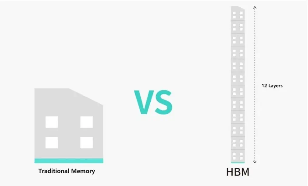
A large 120x120mm chip with 12 HBM4E stacks.
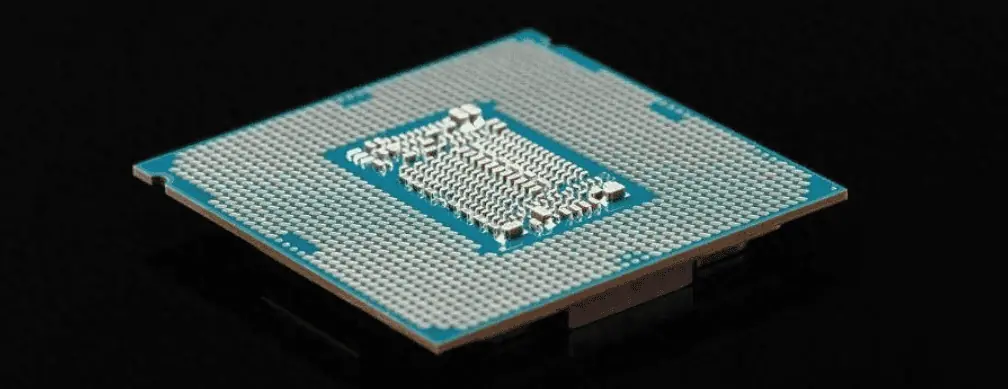
Do you think AMD’s Instinct MI300X and Nvidia’s B200 are large-area GPUs? Think again: TSMC is developing a version of its Chip-on-Wafer-on-Substrate (CoWoS) packaging technology that will more than double the size of system-level packages (SiP). The company announced this at its North American technology symposium. These will use gigantic 120x120mm packages and will consume several kilowatts of power.
The latest version of CoWoS allows TSMC to build a silicon interposer layer about 3.3 times larger than the conventional photomask size (858mm²). As a result, the logic circuits, 8 HBM3/HBM3E memory stacks, I/O, and other small chips can occupy up to 2831mm². AMD’s Instinct MI300X and Nvidia’s B200 utilize this technology, although Nvidia’s B200 processor is larger than AMD’s MI300X.
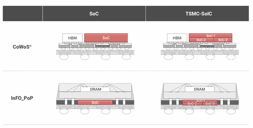
The next generation CoWoS_L will go into production in 2026 and will be able to achieve about 5.5 times the interposer board size of the crosshairs (this might not be as impressive as the six times crosshairs size announced last year). This means 4719 mm² will be available for logic, up to 12 HBM memory stacks, and other small chips. Such SiPs will also require larger substrates; according to TSMC’s slides, we are looking at 100x100mm. Thus, such processors will be unable to use OAM modules.
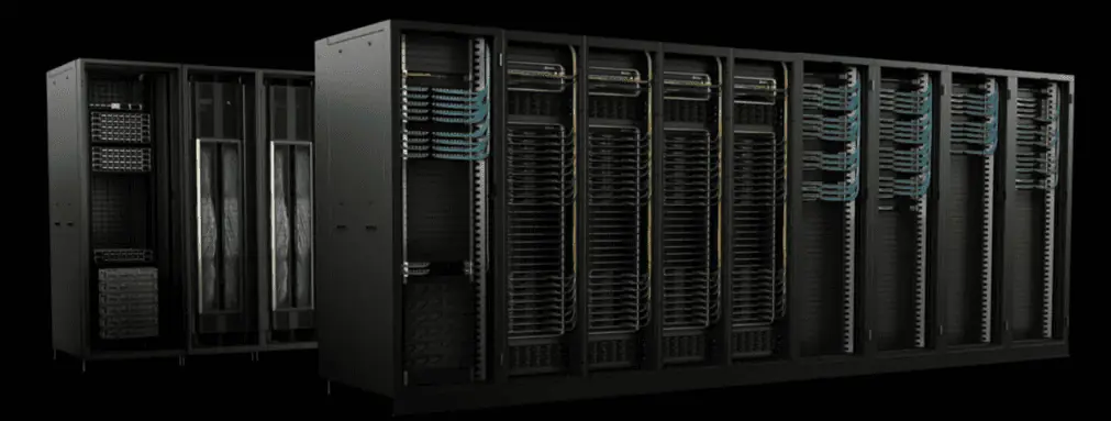
TSMC doesn’t plan to stop there; by 2027, it will have a new version of CoWoS technology that will increase the size of the interposer layer by eight times or more, allowing for a small chip space of 6864 square millimeters. One of TSMC’s envisioned designs relies on four stacked system-level integrated chips (SoIC), paired with 12 HBM4 memory stacks and additional I/O chips. Such a giant will consume a lot of power—we are talking about several kilowatts here, requiring very complex cooling technology. TSMC also hopes such solutions will use a 120x120mm substrate.
Interestingly, earlier this year, Broadcom showcased a custom AI processor with two logic chips and 12 HBM memory stacks. We don’t have the specs, but it looks larger than AMD’s Instinct MI300X and Nvidia’s B200, although it’s not as large as TSMC’s planned for 2027.
02
Introduction to CoWoS Structure and Technology Classification
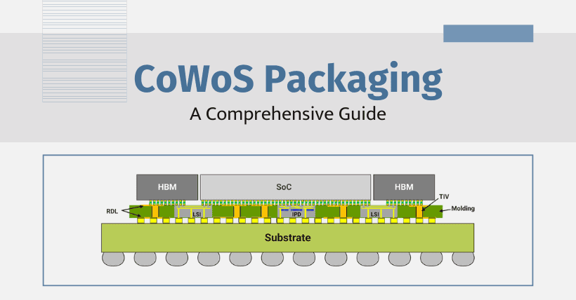
CoWoS (Chip On Wafer On Substrate) is a 2.5D advanced packaging technology from TSMC, derived from the combination of CoW (Chip on Wafer) and oS (on Substrate):
First, the chip is connected to the silicon wafer through the Chip on Wafer packaging process, and then the CoW chip is connected to the substrate, integrating into CoWoS. The core is to stack different chips on the same silicon interposer layer to achieve multi-chip interconnect. In the silicon interposer, TSMC uses technologies such as micro bumps (μBmps) and Through-Silicon Vias (TSV), replacing traditional wire bonding for bare-chip interconnects, significantly enhancing interconnect density and data transmission bandwidth. CoWoS technology improves system performance, reduces power consumption, and reduces packaging size, laying the foundation for TSMC to maintain its lead in subsequent packaging technologies.

Based on the different types of interposers used, TSMC categorizes CoWoS packaging technology into three types—CoWoS-S, CoWoS-R, and CoWoS-L.
CoWoS-S (Silicon Interposer) first appeared in 2011, using a silicon (Si) substrate as an advanced packaging technology (chip-on-wafer-on-substrate with a silicon interposer). It provides a wide range of interposer sizes, HBM cube numbers, and packaging sizes, capable of achieving more than 2X the photomask size (1,700mm2), with the interposer integrating leading SoC chips and four or more HBM2/HBM2E cubes. Traditionally, “CoWoS” referred to advanced packaging technology using a silicon substrate as the interposer.
CoWoS-S evolved from its first generation in 2011 to the fifth generation in 2021, with the sixth generation expected to launch in 2023, which will package 2 compute cores on the substrate and accommodate up to 12 HBM cache chips. The fifth generation of CoWoS-S technology utilized a new TSV solution, thicker copper connections, and twenty times the number of transistors compared to the third generation. Its silicon interposer expanded to 2500mm2, equivalent to three times the photomask area, accommodating space for 8 HBM2E stacks with a capacity of up to 128 GB. Additionally, TSMC provides the latest high-performance processor cooling solution in the form of Metal Tim, reducing the packaging thermal resistance to 0.15 times compared to the first-generation Gel TIM.
CoWoS-R (RDL Interposer) is an advanced packaging technology that uses an organic substrate/re-distribution layer (RDL) instead of silicon (Si) as the interposer. CoWoS-R employs InFO technology using RDL as the interposer and services interconnect between chiplets, particularly in HBM (high bandwidth memory) and SoC heterogeneous integration. The RDL interposer consists of polymers and copper wiring, offering relatively high mechanical flexibility, which enhances the integrity of C4 joints and allows new packages to expand their sizes to meet more complex functional requirements.
CoWoS-L uses chiplets and RDL as the interposer (silicon bridge), combining the advantages of CoWoS-S and InFO technologies with flexible integration. CoWoS-L uses the interposer with LSI (local silicon interconnect) chips for chip-to-chip interconnects, as well as the RDL layer for power and signal transmission. Starting from 1.5 times the reticle interposer size and 1x SoC+4x HBM cubes, it will expand forward to increase the envelope to larger sizes, integrating more chips.
The main functions served by CoWoS-L include: first, LSI chips for high wiring density interconnects through multi-layer submicron copper lines. LSI chips can have various connection architectures in each product (e.g., SoC to SoC, SoC to chiplet, SoC to HBM), and can be reused across multiple products. The corresponding metal types, layers, and spacing are consistent with those of CoWoS-S products. Second, a molded interposer with wide-spacing RDL layers on both front and back, and TIVs (through-interposer vias) for signal and power transmission, providing low high-frequency signal loss in high-speed transmissions. Third, the ability to integrate other components beneath the SoC chip, such as independent IPDs (integrated passive devices), to support better PI/SI signal communication.

Disclaimer: This article is created by the original author. The content of the article represents their personal opinions. Our reposting is for sharing and discussion purposes only and does not imply our endorsement or agreement. If you have any objections, please contact us through the provided channels.


