
High numerical aperture EUV lithography is widely regarded as the next-generation development direction of EUV lithography.
In theory, increasing the numerical aperture (NA) from 0.33 to 0.55 would reduce the absolute minimum half-pitch by 40%, from 10 nanometers to 6 nanometers. However, for extreme ultraviolet systems, it is important to recognize that extreme ultraviolet light (composed of photons) is ionizing, meaning it releases photoelectrons in the absorbing material. Once absorbed, a 92 eV extreme ultraviolet photon generates a photoelectron of about 70-80 eV, gradually depositing most of the energy of the original photon. The density of migrated photoelectrons ultimately replaces the image information originally contained in the density of extreme ultraviolet photons. The positions to which all the photoelectrons eventually migrate determine the difference between the minimum resist exposure and the maximum resist exposure. Additionally, randomness in photon absorption leads to randomness in the number of photoelectrons generated. The random effects of roughness result in rough, unpredictable edge position shifts, and even defects. Considering all these factors, a reevaluation of the practical resolution of extreme ultraviolet lithography is necessary.
01
Photoelectron Model Details
The extreme ultraviolet (EUV) light reaching the chip consists of two components: one is transverse magnetic (TM) polarized light parallel to the incident surface, and the other is transverse electric (TE) polarized light perpendicular to the incident surface. Photoelectrons mainly emit along the polarization direction. Pure unpolarized light should be a 50-50% mixture, but we may have some deviation because mirrors in EUV systems may reflect near Brewster’s angle. Regarding the lines being imaged, photoelectrons along the TE polarization move along the lines, while those along the TM polarization move perpendicular to the lines. Only the latter reduces imaging quality. The lateral movement of photoelectrons effectively shifts the image. Figure 1 shows the relative probability of photoelectron movement to a distance corresponding to a 3 eV cutoff point. This cutoff point corresponds to the thickness loss of the resist after exposure and development.
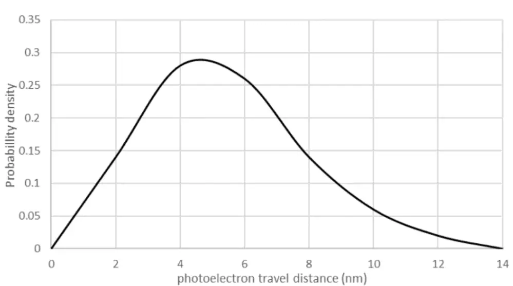
The exposure of resist at a specific point will be influenced by photoelectrons from a specific distance, with the weighted probability density applicable only to the TM case. The TE portion is not affected by the movement of photoelectrons along the lines.
02
Depicting the Diffusion of Optoelectrons.
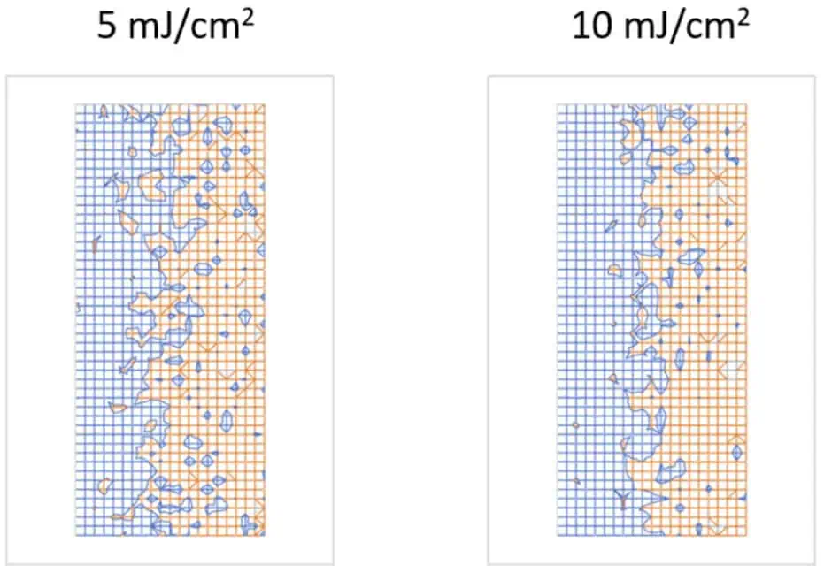
Previous research has found that when the spacing decreases to below 40 nm, the normalized image log slope (NILS) representing image contrast decreases due to photoelectron diffusion. For reference, Figure 2 illustrates the situation of photoelectron diffusion with a spacing of 40 nanometers. The absorbed photon dose is influenced by shot noise, which directly affects the number of generated photoelectrons. At 5 mJ/cm2, the photon dose absorbed by a 40 nm thick organic chemically amplified resist (CAR) is approximately 30 mJ/cm2. Areas nominally unexposed are penetrated by photoelectrons, potentially printing defects, while areas nominally exposed are thoroughly penetrated by photoelectrons, printing gaps. Increasing the dose can reduce the severity of this randomness.
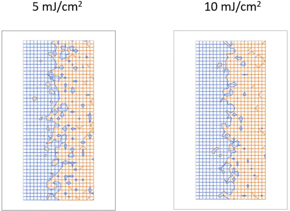
When the spacing increases to 50 nanometers (Figure 3), photoelectrons seem to not diffuse randomly as far, especially at higher doses. This is due to increased contrast, i.e., the separation between maximum and minimum photoelectron densities in the image.
03
Reassess the Direction of Extreme Ultraviolet Lithography Resolution.
The probability density function of EUV photoelectron diffusion shown in Figure 1 indicates that for a typical CAR, under conditions of approximately 30 mJ/cm2, the practical resolution limit is around a 50 nm pitch; under conditions of approximately 90 mJ/cm2, the practical resolution limit is a 40 nm pitch. This is significantly higher than the expected resolution limits of 0.33 or 0.55 NA. Therefore, the resolution limit should not primarily be attributed to the optical technology of EUV systems, but rather to the migration of photoelectrons and secondary electrons within the EUV resist.
Furthermore, resolution is closely related to the dose absorbed by the resist; the higher the dose, the higher the resolution. This leads to a trade-off in throughput, necessitating higher source power compensation. Calibration through low-energy electron scattering simulations and measurements of resist thickness loss and electron dose is necessary to determine the resolution of a specific EUV resist.
It must be noted that while metal-containing resists are known to have enhanced EUV absorption capabilities, tin oxide-based resists may not necessarily have an advantage in terms of photoelectron diffusion distance compared to organic CARs. Limitations on elemental composition will prevent significant deviations in the photoelectron diffusion function. As the resist will be the primary determinant of EUV lithography resolution, the focus on high-NA marketing should be reduced.
Related:
- Future of Earth: Supercomputer Predicts Human Extinction
- How Lithography Powers Advanced Semiconductor Nodes?

Disclaimer: This article is created by the original author. The content of the article represents their personal opinions. Our reposting is for sharing and discussion purposes only and does not imply our endorsement or agreement. If you have any objections, please contact us through the provided channels.


