In the semiconductor industry chain, particularly in the third-generation semiconductor (wide bandgap semiconductor) industry chain, there is a distinction between the substrate and the epitaxial layer. What is the significance of the existence of the epitaxial layer? What is the difference between it and the substrate?

In the wafer preparation process, there are two core steps: one is the preparation of the substrate, and the other is the implementation of the epitaxial process. The substrate, a wafer made from a single crystal semiconductor material, can be directly used in the wafer manufacturing process to produce semiconductor devices, or it can undergo an epitaxial process to enhance performance.
So, what is epitaxy? Simply put, epitaxy is the growth of a new single-crystal layer on a finely processed (cut, ground, polished, etc.) single-crystal substrate. This new single-crystal layer can be the same material as the substrate or a different material, allowing for homoepitaxy or heteroepitaxy as needed. Since the newly grown single-crystal layer extends according to the crystal phase of the substrate, it is called an epitaxial layer. Its thickness is usually only a few micrometers. For example, in silicon, silicon epitaxial growth is the growth of a new single-crystal silicon layer on a silicon single-crystal substrate with a specific crystal orientation, where the resistivity and thickness are controllable and the lattice structure is perfect. Once the epitaxial layer grows on the substrate, the whole is called an epitaxial wafer.
For the traditional silicon semiconductor industry, directly making high-frequency high-power devices on silicon wafers encounters technical challenges, such as meeting the requirements of high breakdown voltage in the collector region, low series resistance, and low saturation voltage drop. The introduction of epitaxial technology cleverly solves these problems. The solution is to grow a high-resistivity epitaxial layer on a low-resistivity silicon substrate, and then make devices on the high-resistivity epitaxial layer. This way, the high resistivity epitaxial layer provides high breakdown voltage for the device, while the low resistivity substrate reduces the resistance of the substrate, thereby lowering the saturation voltage drop, achieving a balance between high breakdown voltage, low resistance, and low voltage drop.
In addition, vapor phase epitaxy, liquid phase epitaxy, and other epitaxial technologies of III-V, II-VI, and other molecular compound semiconductor materials such as GaAs have also greatly developed. These technologies have become essential in manufacturing most microwave devices, optoelectronic devices, and power devices. Especially the successful application of molecular beam epitaxy (MBE) and metal-organic chemical vapor deposition (MOCVD) in thin layers, superlattices, quantum wells, strained superlattices, and atomic-scale thin layer epitaxy has laid a solid foundation for the new field of semiconductor research called “band engineering.”
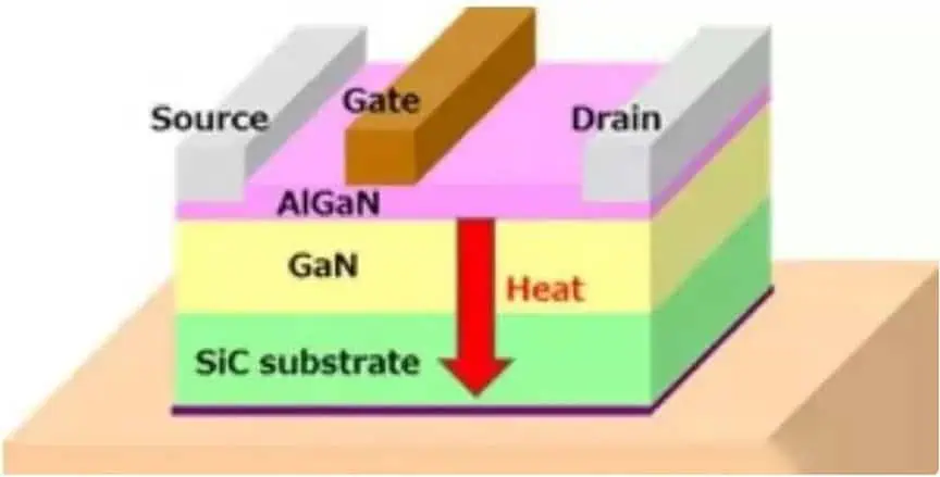
For third-generation semiconductor devices, almost all are made on epitaxial layers, with the silicon carbide wafer itself only serving as the substrate. The parameters of the SiC epitaxial material, such as thickness and background carrier concentration, directly determine the various electrical properties of the SiC device. High-voltage applications of silicon carbide devices impose new requirements on the thickness and background carrier concentration of the epitaxial material. Therefore, silicon carbide epitaxial technology is crucial for fully exploiting the performance of silicon carbide devices. Almost all SiC power devices are prepared based on high-quality SiC epitaxial wafers, and the production of epitaxial layers is an important part of the wide bandgap semiconductor industry.
Epitaxy can be divided into homoepitaxy and heteroepitaxy. Homoepitaxy is the growth of an epitaxial layer of the same material on the substrate. What is the significance of homoepitaxy? It improves product stability and reliability. Although homoepitaxy involves growing an epitaxial layer of the same material on the substrate, it can enhance the purity and uniformity of the material on the wafer surface. Compared to mechanically polished wafers, substrates that have undergone epitaxial treatment have higher surface flatness, higher cleanliness, fewer micro-defects, and fewer surface impurities, resulting in more uniform resistivity. It is also easier to control defects such as surface particles, stacking faults, and dislocations. Epitaxy not only improves product performance but also ensures product stability and reliability.

The so-called first, second, third, and fourth generations of semiconductors are classified based on the material of the substrate or epitaxy. That is, as long as you use the new generation of materials, whether as a substrate or epitaxy, you can claim to be a new-generation semiconductor. For example, if you use single-crystal silicon as a substrate and then grow a GaN epitaxial layer on it, since GaN is used in the material, silicon-based GaN is also considered a third-generation semiconductor.
Further reading:
How are chips classified and what is their relationship to the first, second, third, and fourth generations?
First-generation semiconductors:
Representative materials: Silicon (Si), Germanium (Ge).
Disadvantages of Germanium: Poor thermal stability.
The appearance of germanium transistors in 1948 led to rapid development from 1950 to the early 1970s. Thereafter, they were gradually phased out in developed countries. By 1980, with the maturation of high-purity silicon manufacturing processes, germanium transistors were almost completely replaced by silicon transistors worldwide.
Second-generation semiconductors:
Representative materials: Gallium arsenide (GaAs), Indium phosphide (InP).
Advantages:
- High electron mobility.
- Direct bandgap, making them highly efficient in optoelectronic applications because electrons can transition directly while releasing photons, such as in LEDs and lasers.
Third-generation semiconductors:
Representative materials: Silicon carbide (SiC), Gallium nitride (GaN), Zinc selenide (ZnSe).
Advantages: They have a wide bandgap, high breakdown voltage, and high thermal conductivity. Suitable for high-temperature, high-power, and high-frequency applications.
Fourth-generation semiconductors:
Ga2O3 single crystal substrate.
Representative materials: Gallium oxide (Ga2O3), Diamond (C), Aluminum nitride (AlN), and Boron nitride (BN).
Advantages: Ultra-wide bandgap, high breakdown voltage, high carrier mobility.
Disadvantages: Difficult material growth and preparation; immature manufacturing processes, with many key technologies yet to be fully developed.

Disclaimer: This article is created by the original author. The content of the article represents their personal opinions. Our reposting is for sharing and discussion purposes only and does not imply our endorsement or agreement. If you have any objections, please get in touch with us through the provided channels.


