The author encourages originality, and this article is shared for technical discussion only.
The technical implementation process of PCB cloning can be briefly described as follows: First, the circuit board to be copied is scanned to record the detailed positions of the components. Then, the components are removed to create a Bill of Materials (BOM), and materials procurement is arranged. The bare board is scanned into images, which are processed by copying software to restore it into a PCB layout file. The PCB file is then sent to a manufacturer for production. Once the board is made, the purchased components are soldered onto the newly manufactured PCB board, followed by circuit board testing and debugging.
01
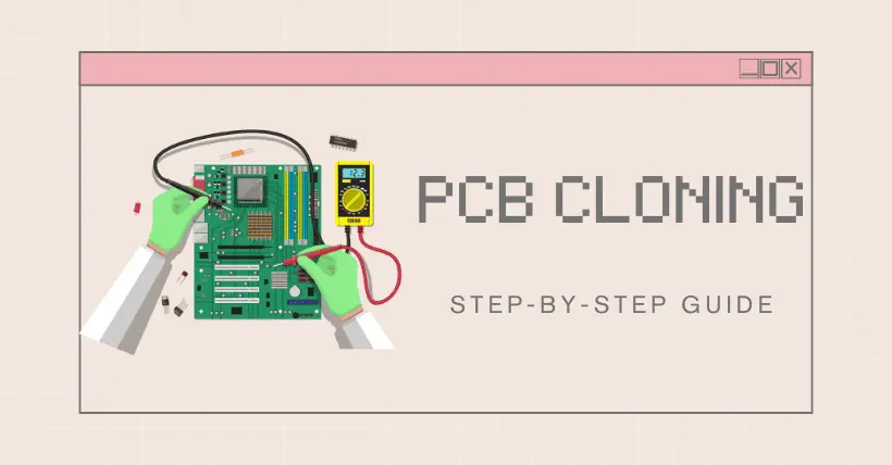
Detailed Steps of PCB Cloning
- Obtain a PCB, and first record all component models, parameters, and positions on paper, especially noting the orientation of diodes, transistors, and the direction of IC notches. It’s best to take a few photos of the component placements with a digital camera, as modern PCB boards often have components like diodes and transistors that are difficult to see clearly.
- Remove all components from the board and remove any solder from the PAD holes. Clean the PCB thoroughly with alcohol, then place it in a scanner. Adjust the scanner’s resolution to a higher setting for clearer images. Lightly polish the top and bottom layers with fine sandpaper until the copper film shines, then scan each layer separately in color using Photoshop. Ensure that the PCB is positioned squarely in the scanner to avoid skewed images.
- Adjust the contrast and brightness of the scanned image so that the areas with and without copper film have strong contrast, then convert the image to black and white. Check the clarity of the lines; if unclear, repeat this step. Once clear, save the image as a black-and-white BMP file, naming the files TOP.BMP and BOT.BMP. If there are issues, corrections can be made using Photoshop.
- Convert the two BMP files into PROTEL format files. Import both layers into PROTEL and check that the positions of PADs and VIAs align; if they do, previous steps were done well. If there’s a misalignment, repeat Step 3. PCB copying requires patience as even small errors affect quality and alignment.
- Convert the BMP file of the TOP layer to TOP.PCB, ensuring it’s converted to the SILK layer (yellow). Then, trace the lines on the TOP layer, placing components according to Step 2’s records. After drawing, delete the SILK layer and repeat until all layers are complete.
- Import both TOP.PCB and BOT.PCB into PROTEL and merge them into a single file.
- Use a laser printer to print the TOP and BOTTOM layers onto transparent films (1:1 ratio). Align the films with the PCB and check for errors. If everything matches, the copying process is complete.
A replica PCB identical to the original has now been created, but this is only half the process. The electronic performance of the copied board must be tested to ensure it matches the original. If it performs the same, the copying process is complete.
Note: For multilayer boards, carefully polish down to the inner layers and repeat steps 3 to 5 for each layer. Layer names vary based on the number of layers, and double-sided boards are typically simpler to copy than multilayer boards, where alignment issues can easily arise. Multilayer PCB copying requires special attention, particularly to ensure alignment of conductive and non-conductive vias.
02
Double-Sided PCB Copying Method
- Scan the top and bottom layers of the PCB, saving two BMP images.
- Open the PCB copying software Quickpcb2005, click “File” and then “Open Background” to open one of the scanned images. Use PAGEUP to zoom in until the pads are visible. Press PP to place a pad when you see one, and PT to trace lines as they appear—similar to tracing. Save the drawing to generate a B2P file.
- Click “File” and “Open Background” again to open the other layer’s scanned image.
- Next, click “File” and “Open” to open the previously saved B2P file. The copied board will now be overlaid onto this new image—the same PCB, with the holes in the same positions, but with different circuit connections. Select “Options” and “Layer Settings” to hide the top layer’s lines and silkscreen, leaving only the multilayer vias visible.
- With the vias on the top and bottom layers aligned, trace the bottom layer’s circuits in the same way. Then click “Save”—the B2P file will now contain both the top and bottom layers.
- Click “File” and “Export as PCB File” to generate a PCB file with both layers, ready for further editing, schematic generation, or direct submission to a PCB manufacturer.
03
Multilayer PCB Copying Method
Copying a four-layer board essentially involves duplicating the process for two double-sided boards, while a six-layer board means copying three double-sided boards, and so on. Multilayer boards can be challenging due to their hidden internal traces. To access these, “layer separation” is required.
Various methods exist for layer separation, such as chemical etching and tool scraping, but these often risk overdoing it and losing data. The most accurate method, based on experience, is sanding with sandpaper.
After copying the top and bottom layers of the PCB, sandpaper is typically used to gradually remove each layer, revealing the inner traces. Standard sandpaper from hardware stores works well. Place the PCB flat, and sand it evenly. If the board is small, you can place the sandpaper flat and rub the PCB across it with your finger. The key is to keep it flat to ensure uniform sanding.
The silkscreen and green solder mask usually come off with a few rubs, while copper traces require a bit more effort. Generally, small Bluetooth boards can be sanded in a few minutes, while memory modules might take ten minutes or more, depending on the amount of pressure applied.
Sanding is the most common and economical way to separate layers. You can try it on a discarded PCB first; while it can be tedious, there’s no risk of sanding through the board or damaging your fingers.
After the PCB layout is complete, review the design to ensure optimal system layout. Evaluate the following:
- System Layout: Ensure routing is logical or optimal, capable of reliable performance, and that circuit operation is dependable. During layout, plan the signal paths, as well as the power and ground networks, to maintain an overall understanding and strategic layout.
- Board Dimensions: Verify that the PCB dimensions match the specifications on the fabrication drawings and meet manufacturing standards. Often, an otherwise well-designed board may be unusable due to overlooked connector alignment, preventing proper interfacing with other circuits.
- Component Spacing: Ensure there are no conflicts in the 2D or 3D space for component placement, especially in terms of component height. Typically, unseated components should not exceed 3mm in height.
- Component Arrangement: Check that components are orderly and all positioned, with a balanced layout. Consider the signal paths, types, and sensitive areas, while also distributing components evenly.
- Replaceable Parts Accessibility: Confirm that frequently replaced components are easy to access for replacement, and that the board can be conveniently inserted into or removed from devices.
Related:
- SK Hynix Strategic Approach to Maintaining Competitiveness
- Intel Four CEOs Leave the Company in Turmoil and Chaos

Disclaimer:
- This channel does not make any representations or warranties regarding the availability, accuracy, timeliness, effectiveness, or completeness of any information posted. It hereby disclaims any liability or consequences arising from the use of the information.
- This channel is non-commercial and non-profit. The re-posted content does not signify endorsement of its views or responsibility for its authenticity. It does not intend to constitute any other guidance. This channel is not liable for any inaccuracies or errors in the re-posted or published information, directly or indirectly.
- Some data, materials, text, images, etc., used in this channel are sourced from the internet, and all reposts are duly credited to their sources. If you discover any work that infringes on your intellectual property rights or personal legal interests, please contact us, and we will promptly modify or remove it.


