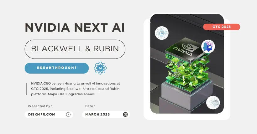
Tomorrow, NVIDIA’s founder and CEO Jensen Huang will have a crucial opportunity to revitalize the company’s stock price. At NVIDIA’s annual technology conference, GTC, Huang will outline how he is leading NVIDIA to explore the next frontier of AI.
According to previous forecasts from JPMorgan, NVIDIA is expected to unveil the Blackwell Ultra chip (GB300) at the conference and may disclose some details about the Rubin platform. The conference will also focus on a comprehensive upgrade of AI hardware, including higher-performance GPUs, HBM memory, enhanced cooling and power management, and the roadmap for CPO (co-packaged optics) technology.
Ahead of Huang’s keynote speech, let’s take a look at the series of architectures NVIDIA has introduced over the years and the stories behind them.
At the end of 1999, NVIDIA launched its first GPU (Graphics Processing Unit), the GeForce 256, integrating a complete rendering pipeline into hardware and providing a solid acceleration effect. However, this product could hardly be called a processor at the time, as it lacked any programmability. It was not until 2001, with the introduction of programmable vertex shaders in DirectX 8, that NVIDIA added the Vertex Processor to the GeForce 3, making the GPU programmable. Subsequently, more programmable shaders were introduced through DirectX and OpenGL to meet the algorithmic needs of rendering developers.
Initially, GPUs were designed for graphics acceleration rather than deep learning. Before NVIDIA introduced the CUDA architecture, GPUs had limited support for deep learning computations. The GPUs truly used for AI computing are not ordinary graphics cards but GPGPUs (General-Purpose Computing on Graphics Processing Units), designed for non-specific (general-purpose) computational workloads.
01
The Beginning of a Revolution: The Birth of CUDA Architecture
As GPUs gained programmability, their potential for parallel computing was discovered. At the time, many universities and research institutions were experimenting with using GPUs for scientific computing.
At SIGGRAPH 2003, several industry pioneers presented ideas and experimental models for using GPUs for various computations. The conference even arranged discussions on GPGPU. However, developers at the time could only use shader programming languages, which required mapping computational resources into rendering concepts, making it cumbersome. This created an urgent need for a programming language specifically designed for GPU parallel computing.
Ian Bark, a PhD student at Stanford at the time, recognized this need and joined the development of Brook, a parallel computing programming language later acquired by AMD. He became an early pioneer in GPU parallel computing software stacks. In 2004, he interned at NVIDIA and, two years later, developed CUDA.
As rendering demands diversified and parallel computing was budding, the Tesla G80 architecture was designed in this historical context, marking a crucial turning point for NVIDIA.
In 2006, NVIDIA launched the first-generation Tesla architecture (G80), initiating the exploration of general-purpose GPU computing. While previous graphics cards had gone through multiple generations, they were primarily for graphics processing. The Tesla architecture introduced the CUDA framework, allowing GPU programming with C language for general-purpose parallel computing. This marked a pivotal moment in NVIDIA’s transformation.
Tesla G80 was the first GPGPU to implement the CUDA architecture, ushering in an era of parallel acceleration. It was one of the most significant GPU innovations in history, with the first products, GeForce 8800 GTX/GTS, released in November 2006. NVIDIA then introduced the second-generation Tesla architecture (GT200), whose double-precision FMA computation speed reached 30 FMA ops/clock—an eightfold increase.
Over about three years with the G80-G200 series, NVIDIA gathered extensive user feedback and recruited Bill Dally as Chief Scientist. This led to the development of the groundbreaking Fermi architecture, the first to feature L1 cache and ECC error correction, designed for supercomputers. The launch event featured several key figures from the supercomputing industry, signaling NVIDIA’s ambitions in the field.
In 2010, NVIDIA officially introduced the Fermi architecture, not just as a hardware update but as the first GPU designed specifically for computational tasks. In redefining GPUs, NVIDIA aimed to accelerate parallel computing while maintaining strong graphics rendering capabilities. The first Fermi-based GPU, GF100, packed 3 billion transistors and was optimized for next-gen gaming and general computing, supporting all DirectX 11 features, including tessellation and compute shaders.
G80 was the initial vision of a unified graphics and computing processor. GT200 expanded G80’s performance and functionality. GF100, optimized for next-gen gaming and general-purpose applications, demonstrated NVIDIA’s commitment to parallel computing. If Tesla G80 was NVIDIA’s first step, Fermi marked the full-scale entry into the computing industry.
02
NVIDIA’s High-Performance Computing Strategy
Afterward, NVIDIA maintained an approximately two-year cycle for new architectures, continuously innovating.
In 2012, NVIDIA launched the Kepler architecture, the first to support supercomputing and double-precision computing. Thanks to 28nm process technology, Kepler significantly improved performance and power efficiency. The Kepler GK110 had 2,880 streaming processors and 288GB/s bandwidth, delivering 3-4 times the computational power of Fermi. With Kepler, GPUs became a key focus in high-performance computing.
In 2014, NVIDIA introduced Maxwell, an upgrade from Kepler, using TSMC’s 28nm process. The rise of mobile devices drove demand for low-power, high-performance GPUs adaptable to different scenarios, leading to Maxwell’s development. The first Maxwell-based GPU, GM107, was designed for power-limited environments like laptops and small form-factor PCs. It featured 1.87 billion transistors and a newly designed SMM (Streaming Multiprocessor) structure, boosting per-core efficiency by 35% and doubling power efficiency. The first GM107-based graphics card was the GeForce GTX 750 Ti.
In 2016, NVIDIA released the Pascal architecture, the successor to Maxwell, using 16nm FinFET technology, HBM2, and NVLink. It was the first GPU designed specifically for deep learning, supporting all major deep learning frameworks. Pascal GPUs, such as GP100 (3,840 CUDA cores, 60 SM units) and GP102 (3,584 CUDA cores, 28 SM units), offered exceptional power. The GP100 provided 732GB/s memory bandwidth while consuming only 300W—over 50% more efficient than Maxwell.
At the time, deep learning was booming, with specialized neural network accelerators outperforming GPUs in efficiency and density. To stay competitive, NVIDIA broke its usual two-year architecture update cycle, launching the Volta architecture the following year.
Volta introduced Tensor Cores to accelerate matrix operations and improve deep learning efficiency. It also supported NVLink 2.0 for faster multi-GPU communication. The Volta GV100 featured 5,120 CUDA cores, 900GB/s bandwidth, and 640 Tensor Cores, delivering 112 TFLOPS of AI performance—nearly triple Pascal’s. This marked a shift toward AI-focused GPU development.
03
NVIDIA Leads the AI Era
In 2016, Jensen Huang personally delivered the first DGX-1 supercomputer to OpenAI. By late 2022, OpenAI’s release of ChatGPT showcased groundbreaking natural language processing capabilities, marking a milestone in deep learning. As the AI revolution surged, NVIDIA introduced the H100 GPU, powered by the Hopper architecture, becoming the world’s most powerful parallel processor.
H100, NVIDIA’s ninth-generation data center GPU, integrates 80 billion transistors, optimized for large-scale AI and HPC computing. Hopper introduced FP8 Tensor Cores for faster AI training and inference. Notably, Hopper removed RT Cores to allocate more resources to deep learning. It also featured a Transformer Engine, excelling in Transformer-based models.
The NVIDIA Grace Hopper Superchip combines Hopper GPUs with NVIDIA Grace CPUs via high-bandwidth NVLink-C2C interconnect, offering up to 900GB/s data transfer rates.
In 2024, NVIDIA’s Blackwell architecture brought generative AI to new heights. The GB200 Superchip delivers up to 30x performance in LLM inference compared to H100 while improving energy efficiency by 25x. Blackwell pairs two GPUs with Grace CPUs, featuring second-gen Transformer Engines for FP4 and FP6 support, optimizing memory and bandwidth usage. Fifth-gen NVLink doubled GPU bandwidth to 1,800GB/s.
With its continuous AI-focused innovations, NVIDIA is redefining the boundaries of deep learning. As Jensen Huang stated last year, NVIDIA engineers are developing the next two generations, aiming for annual architectural advancements.
Tomorrow, NVIDIA’s next breakthrough awaits.
Source: Internet
Related:

Disclaimer:
- This channel does not make any representations or warranties regarding the availability, accuracy, timeliness, effectiveness, or completeness of any information posted. It hereby disclaims any liability or consequences arising from the use of the information.
- This channel is non-commercial and non-profit. The re-posted content does not signify endorsement of its views or responsibility for its authenticity. It does not intend to constitute any other guidance. This channel is not liable for any inaccuracies or errors in the re-posted or published information, directly or indirectly.
- Some data, materials, text, images, etc., used in this channel are sourced from the internet, and all reposts are duly credited to their sources. If you discover any work that infringes on your intellectual property rights or personal legal interests, please contact us, and we will promptly modify or remove it.


