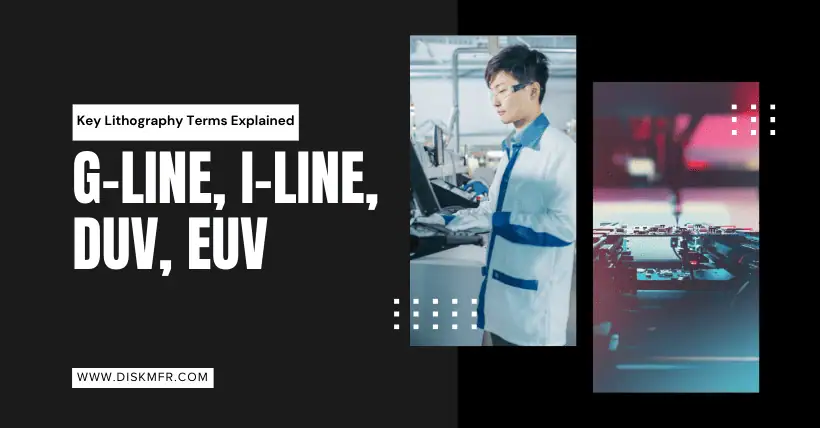
Different wavelength light sources correspond to different technology nodes and manufacturing requirements. From the early G-line and I-line to the current mainstream KrF, ArF, and the cutting-edge EUV, each upgrade has showcased higher resolution and more advanced process levels. As device sizes continue to approach the physical limits, EUV and its subsequent upgraded versions will continue to develop.
However, it is important to note that EUV equipment is expensive and maintenance is complex. Additionally, supporting technologies such as mask technology, substrate materials, and photoresists must also be improved in tandem. Therefore, there is widespread demand in the industry for flexible transition solutions such as multiple exposure and hybrid processes (combining ArF and EUV). In the future, there may be breakthroughs with even shorter wavelengths or new technologies based on electron beams, but to achieve large-scale mass production, many engineering and cost challenges still need to be gradually overcome.
I. Background and Importance in semiconductor lithography processes
In the chip manufacturing process, photolithography is considered the core step in determining the integration level of integrated circuits, with the main goal of “printing” the designed micro-nano circuit patterns onto the substrate (usually silicon wafers). As the demand for chip miniaturization and performance improvement grows increasingly urgent, the photolithography resolution has continuously evolved. Whether the resolution can be further improved largely depends on the wavelength of the light source used—shorter wavelengths allow for higher potential resolution, thus meeting the demands of more advanced and refined technology nodes.
II. Correspondence Between Light Source Wavelength and Technology Nodes
✅ Ultraviolet Light (Mercury Lamps)
G-line (436 nm) corresponding technology node: ≥0.5 µm. Applicable scenarios: Early integrated circuit manufacturing or devices with low line-width requirements. Characteristics: Stable and mature process, relatively low equipment cost, but unable to meet the linewidth demands of deep submicron levels.
I-line (365 nm) corresponding technology node: 0.35–0.25 µm. Applicable scenarios: A more advanced generation of ultraviolet photolithography technology than G-line, widely used in 0.35 µm and 0.25 µm nodes. Characteristics: Once the mainstream solution for large-scale production, but now largely replaced by deep ultraviolet processes in higher-end fields.
✅ Deep Ultraviolet (DUV)
KrF (248 nm) corresponding technology node: 0.25–0.13 µm. Applicable scenarios: Mainstream photolithography technology in the submicron domain, pushing the integrated circuit process to the 0.13 µm threshold. Characteristics: The shorter wavelength compared to I-line improves photolithography resolution and enables processes such as single-layer and multi-layer mask exposure.
ArF (193 nm / Immersion 193 nm) corresponding technology node: 0.13 µm–7 nm. Applicable scenarios: From 0.13 µm down to smaller nodes, including tens of nanometers and even several nanometers, many high-end processes rely on ArF combined with immersion and multiple exposure techniques. Characteristics: The 193 nm light source, combined with immersion technology, can “effectively” increase the numerical aperture (NA) of the exposure system, further enhanced by dual/multiple exposures, covering a very wide node range. Many advanced fabs still use ArF immersion lithography and multiple exposures in the 7 nm or 10 nm process.
F₂ (157 nm) corresponding technology node: Not yet industrialized. Applicable scenarios: Theoretically capable of achieving high resolution, but facing bottlenecks in materials, optical systems, and costs, it has not been mass-produced. Characteristics: Once seen as the next-generation deep ultraviolet lithography potential solution, but due to many technical challenges, it has been partially replaced by EUV technology.
✅ Extreme Ultraviolet (EUV)
EUV (13.5 nm) corresponding technology node: 7 nm/5 nm and below. Applicable scenarios: Used for the most advanced process nodes (7 nm, 5 nm, and even 3 nm, 2 nm), a key technology for high-performance processors and advanced memory chips. Characteristics: The wavelength is much shorter than DUV, but it places extremely high demands on the optical system, vacuum environment, mask, and light source generation methods, making equipment and operational costs expensive. The introduction of EUV significantly reduces the need for multiple exposures, helping simplify the process flow and improve overall yield.
III. Basic Principles of Light Source Wavelength and Resolution
Photolithography resolution is typically quantified using a formula similar to the Rayleigh Equation, simplified as:
In this equation, λ represents the wavelength of the light source, and NA (numerical aperture) represents the performance of the optical system. The shorter the wavelength, the smaller the minimum linewidth that can be imaged; similarly, increasing NA through immersion photolithography can further reduce the resolution limit. Based on this principle, the industry has continually advanced toward shorter wavelengths to achieve finer linewidths: from traditional G-line and I-line to KrF, ArF, and finally to EUV. This explains the clear “matching” or “correspondence” between light source types and technology nodes.
IV. Other Factors Affecting Light Source Selection
Photolithography system complexity: The shorter the wavelength, the higher the quality of optical components and the more complex the exposure system required. For EUV, it also needs to operate in a vacuum environment, and factors such as light source power and durability are significant challenges.
Materials and photoresists: At different wavelengths, photoresists need to meet specific absorption/transmission characteristics, with significant differences in process windows.
Process costs: More advanced photolithography machines are much more expensive, and maintenance costs are significantly higher, requiring evaluation of mass production scale and chip profit margins.
Multiple exposure and process iterations: For the same light source, multiple exposures (such as dual or triple exposures) can somewhat overcome the physical limits of single exposure. For example, ArF immersion lithography, assisted by multiple exposures, can support down to 7 nm and even some 5 nm processes.
V. Simple Analogy: Light and Focus
Photolithography can be understood as “printing very fine patterns on a film using light”—if the “light” emitted by the lamp is “rough” (long wavelength), the ability to print clear small patterns is limited; if a “finer” light (shorter wavelength) is used, it can capture more delicate “photos” with the same “lens.” In semiconductor processes, the light, camera lens, and film correspond to the light source, optical imaging system, and photoresist/silicon wafer surface, respectively.
VI. Conclusion and Outlook
In conclusion, the wavelength of the light source is a key factor in determining the photolithography resolution and whether technology nodes can successfully advance. As wavelengths continue to shorten and corresponding optical technologies innovate, chip linewidths can continue to shrink, driving the semiconductor industry toward higher performance, lower power consumption, and greater density.
Related:

Disclaimer:
- This channel does not make any representations or warranties regarding the availability, accuracy, timeliness, effectiveness, or completeness of any information posted. It hereby disclaims any liability or consequences arising from the use of the information.
- This channel is non-commercial and non-profit. The re-posted content does not signify endorsement of its views or responsibility for its authenticity. It does not intend to constitute any other guidance. This channel is not liable for any inaccuracies or errors in the re-posted or published information, directly or indirectly.
- Some data, materials, text, images, etc., used in this channel are sourced from the internet, and all reposts are duly credited to their sources. If you discover any work that infringes on your intellectual property rights or personal legal interests, please contact us, and we will promptly modify or remove it.


