I. Related Fundamental Knowledge about PN Junction
A semiconductor is a material whose conductivity lies between that of a conductor and an insulator, with common examples including silicon (Si) and germanium (Ge). A pure semiconductor (also called an intrinsic semiconductor) has equal numbers of charge carriers (including electrons and holes) internally.
At absolute zero, an intrinsic semiconductor behaves like an insulator, with almost no conductivity. However, as the temperature rises, some electrons gain enough energy to break free from covalent bonds, becoming free electrons, while leaving behind a vacancy in the covalent bond—known as a hole. Both free electrons and holes can conduct electricity, which is the basic principle behind intrinsic semiconductor conductivity.
To enhance the conductivity of semiconductors, specific impurities can be introduced into intrinsic semiconductors, resulting in P-type and N-type semiconductors. For example, introducing trivalent elements (such as boron, B) into an intrinsic semiconductor forms covalent bonds with surrounding silicon atoms but lacks one electron, creating a hole. This type of semiconductor, where holes are the majority carriers and electrons are the minority carriers, is called a P-type semiconductor.
Conversely, introducing pentavalent elements such as phosphorus (P) into an intrinsic semiconductor leads to the formation of covalent bonds between phosphorus and silicon atoms, leaving an extra electron. This type of semiconductor is called an N-type semiconductor.
II. Formation of the PN Junction
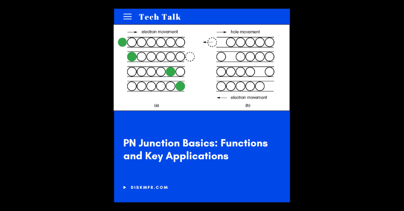
When a P-type semiconductor and an N-type semiconductor are closely joined, the high concentration of holes in the P-type region and the high concentration of electrons in the N-type region cause charge carriers to diffuse from high to low concentration regions. Electrons in the N-type region diffuse toward the P-type side, and holes in the P-type region diffuse toward the N-type side.
This diffusion movement causes changes in the distribution of charge carriers near the interface of the P-type and N-type semiconductors. The P-type side loses holes, leaving behind immobile negative ions, while the N-type side loses electrons, leaving behind immobile positive ions. These immobile charged ions form a space charge region near the interface, which is the prototype of the PN junction.
The formation of the space charge region establishes an internal electric field pointing from the N region to the P region. This internal electric field, on one hand, prevents further diffusion of majority carriers, and on the other hand, promotes the drift movement of minority carriers. Under the influence of the internal electric field, minority carriers drift from the P region to the N region and from the N region to the P region. When diffusion and drift reach dynamic equilibrium, the width of the space charge region stabilizes, and the PN junction is officially formed.
III. Unidirectional Conductivity of the PN Junction
Unidirectional conductivity is the most important characteristic of a PN junction and the basis for the operation of many semiconductor devices. When a forward bias is applied to the PN junction, i.e., the P region is connected to the positive terminal of the power supply and the N region to the negative terminal, the external electric field opposes the internal electric field, weakening it. This narrows the space charge region and intensifies the diffusion of majority carriers, producing a large forward current. Even a slight increase in the external voltage results in a significant rise in the forward current, placing the PN junction in a conducting state.
When a reverse bias is applied to the PN junction, i.e., the P region is connected to the negative terminal and the N region to the positive terminal of the power supply, the external electric field aligns with the internal electric field, strengthening it. The space charge region widens, the diffusion of majority carriers is suppressed, and the drift of minority carriers produces a reverse current. Because the current is very small and hardly changes with increased reverse voltage within a certain range, the PN junction is in a cutoff state.
When the reverse voltage increases beyond a certain point, the PN junction undergoes breakdown, and the reverse current rises sharply. Breakdown is classified into avalanche breakdown and Zener breakdown. Avalanche breakdown commonly occurs in lightly doped PN junctions, while Zener breakdown typically occurs in heavily doped ones.
IV. PN Junction Capacitance
The PN junction exhibits capacitive effects, including barrier capacitance and diffusion capacitance. Barrier capacitance arises from changes in the width of the space charge region with varying applied voltage and is similar to the capacitance of a parallel-plate capacitor. As the applied voltage changes, the amount of charge in the space charge region changes accordingly, producing a capacitive effect.
Diffusion capacitance, on the other hand, occurs when the PN junction is forward-biased. It is generated by the change in accumulated charge of majority carriers during diffusion as the applied voltage varies. In high-frequency applications, the capacitive effect of the PN junction significantly impacts device performance and must be fully considered in circuit design.
V. Applications of the PN Junction
The PN junction has a wide range of applications, with the diode being the most typical example. A diode consists of a PN junction along with appropriate electrode leads and casing. Using the unidirectional conductivity of the PN junction, it can perform rectification, detection, and clamping functions. In power circuits, rectifier diodes convert AC to DC. In radio communications, detector diodes extract low-frequency signals from high-frequency ones.
In addition, PN junctions are widely used in transistors, integrated circuits, and other complex semiconductor devices. In bipolar junction transistors, the interaction of two PN junctions enables current amplification and switching functions. In integrated circuits, numerous PN junctions are embedded within a tiny chip to form various complex circuits, greatly promoting the miniaturization and intelligence of electronic devices.
VI. Author’s Summary
Overall, the PN junction is a very important and central concept in the field of semiconductor physics and a key cornerstone in the development of modern electronic technology. As technology continues to advance, in-depth research into PN junctions will provide a continuous driving force for innovation in semiconductor technology and create more possibilities for the development of human society.
Related:

Disclaimer:
- This channel does not make any representations or warranties regarding the availability, accuracy, timeliness, effectiveness, or completeness of any information posted. It hereby disclaims any liability or consequences arising from the use of the information.
- This channel is non-commercial and non-profit. The re-posted content does not signify endorsement of its views or responsibility for its authenticity. It does not intend to constitute any other guidance. This channel is not liable for any inaccuracies or errors in the re-posted or published information, directly or indirectly.
- Some data, materials, text, images, etc., used in this channel are sourced from the internet, and all reposts are duly credited to their sources. If you discover any work that infringes on your intellectual property rights or personal legal interests, please contact us, and we will promptly modify or remove it.


