The chip is the essence of human technology and is also known as the jewel in the crown of modern industry.
The basic component of a chip is the transistor. The fundamental working principle of a transistor is not actually complicated, but when you cram tens of billions of transistors into an area the size of a fingernail, it becomes no longer simple. It can even be considered one of the most complex engineering feats in human history, without exception.
In the upcoming period, I will introduce the chip manufacturing process through a series of articles.
Today’s article will first talk about wafer manufacturing.
01
█ Major Stages and Divisions of Labor
Before introducing the wafer, let me first provide some background knowledge on chip manufacturing.
Chip manufacturing involves hundreds of processes. We can initially categorize them into four main stages: chip design, wafer preparation, chip manufacturing (front-end), and packaging/testing (back-end).
We often hear terms like Fabless, Foundry, and IDM. These terms are closely related to the division of labor in the chip industry.
Generally speaking, some companies in the industry focus solely on chip design and do not engage in manufacturing, packaging, or testing. These companies are known as Fabless, such as Qualcomm, Nvidia, MediaTek, and (formerly) Huawei.
There are also companies that specialize in chip production without having their own branded chips. These companies are known as Foundries, wafer foundries.
The most famous Foundry is Taiwan’s TSMC. SMIC, UMC, and Hua Hong Group also belong to the Foundry category.
Chip manufacturing is more difficult than chip design. Many companies in our country have advanced chip design capabilities but cannot find a Foundry to produce the chips. Therefore, the so-called “bottleneck” usually refers to the chip manufacturing process.
The chips produced by a Foundry are usually called bare dies. A bare die cannot be used directly and needs to go through packaging, testing, and other steps. Companies that specialize in packaging and testing are called OSAT (Outsourced Semiconductor Assembly and Test).
Of course, some wafer foundries also have their own packaging and testing facilities, but they are generally not as flexible and efficient as OSATs. Well-known OSAT players in the industry include ASE, JCET, UTAC, and Amkor.
Finally, there is IDM.
IDM stands for Integrated Device Manufacturer. Some companies handle chip design, wafer production, and packaging/testing, doing everything from start to finish. These companies are called IDMs.
There are not many companies globally that have this capability, including Intel, Samsung, Texas Instruments, and STMicroelectronics.
IDMs may seem powerful as they do everything, but in reality, the chip industry is too vast, and specialized divisions of labor are the trend. The Fabless + Foundry model has distinct advantages in terms of professionalism, efficiency, and profitability.
AMD used to be an IDM, but later shifted to the Fabless model. After spinning off its wafer foundry, it transformed into GlobalFoundries, one of the top five wafer foundries in the world.
02
█ Wafer Preparation
First, let’s start with the most basic process: wafer preparation.
We often say that chips are made from sand. In fact, this is mainly because sand contains a large amount of silicon (Si) elements.
Silicon is the second most abundant element in the Earth’s crust, second only to oxygen.
Silicon is present in sand, but in low purity and as silicon dioxide (SiO2). We cannot just grab a handful of sand to extract silicon. Typically, quartz sand ore with a higher silicon content is selected.
✅ Step 1: Deoxidization and Purification.
The quartz sand material is placed into a furnace and heated to a temperature above 1400°C (the melting point of silicon is 1410°C). A chemical reaction with a carbon source produces high-purity (over 98%) metallurgical-grade silicon (MG-Si).
Next, the silicon is further purified through chlorination and distillation processes to obtain higher purity silicon.
This silicon material is not only used for semiconductor chip manufacturing but also for the photovoltaic industry (solar power generation).
In the photovoltaic industry, the purity requirement for silicon is 99.9999% to 99.999999%, or 4 to 6 nines, known as SG-Si (solar-grade silicon).
In the semiconductor chip industry, the purity requirement is even more extreme, ranging from 99.9999999% to 99.999999999%, or 9 to 11 nines. This silicon, used for semiconductor manufacturing, is called electronic-grade silicon (EG-Si), where, on average, only one impurity atom is allowed for every million silicon atoms.
✅ Step 2: Pulling Single Crystal Silicon (Casting Ingot)
The silicon obtained after purification is polycrystalline silicon. The next step is to turn it into single crystal silicon.
Earlier, when I introduced the brief history of semiconductor development, I explained the difference between single crystal silicon and polycrystalline silicon.
In simple terms, single crystal silicon has a perfect crystal structure and excellent performance. Polycrystalline silicon has large, irregular grains with many defects and relatively poor performance. Therefore, high-end chips mainly use single crystal silicon, while polycrystalline silicon is used in photovoltaic applications.
The mainstream method to turn polycrystalline silicon into single crystal silicon is the Czochralski method (also known as the pulling method).
First, the high-purity polycrystalline silicon is heated and melted to form liquid silicon.
Then, a small seed crystal of single crystal silicon is dipped into the silicon melt.
Next, the seed crystal is slowly rotated and pulled upward. The silicon melt solidifies into a solid silicon column as it is pulled upward, and the silicon atoms that leave the liquid surface align in an orderly manner, forming a single crystal silicon column.
(Note: The pulling speed varies. Initially, the crystal is pulled at 6mm per minute for about 10 cm, as the crystal structure is unstable due to thermal shock and easily generates defects. After 10 cm, the pulling speed slows down to ensure better quality.)
The speed of pulling and temperature control greatly influence the quality of the silicon ingot. The larger the diameter of the ingot, the more precise the speed and temperature control need to be.
Finally, a cylindrical silicon ingot with a diameter of about 30 cm and a length of 1 to 1.5 meters is pulled. This silicon ingot is called a crystal bar, also known as a silicon ingot.
✅ Step 3: Wafer Cutting.
The pulled silicon ingot has its head and tail cut off and then sliced into thin wafers of a specific thickness.
The mainstream method for slicing wafers is using a multi-wire saw with diamond particles on the wires to cut the silicon ingot into multiple segments. This method is efficient and results in low material loss.
Sometimes, an inner circular saw is also used. This saw has diamond-coated inner circular blades that rotate to slice the silicon ingot. Inner circular saws have higher cutting precision and speed and are suitable for high-quality wafer cutting.
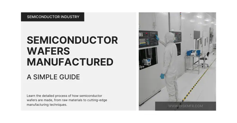
Silicon wafers are fragile, so the cutting process needs to be handled very carefully, with strict control of temperature and vibration. Cutting liquid, either water-based or oil-based, is used to cool, lubricate, and remove debris generated during cutting.
✅ Step 4: Edge Grinding, Polishing, and Cleaning.
The cut silicon wafers, known as “bare wafers,” have very rough surfaces and residual cutting liquid and debris. Therefore, they need to go through edge grinding, polishing, cleaning, and other processes to achieve a smooth, mirror-like surface.
Edge grinding is done with a grinding machine to round off the sharp edges of the wafer. This reduces the risk of breakage due to the brittleness of high-purity silicon.
Polishing is done to smooth out the wafer surface, making it flat and reducing mechanical defects.
After polishing, the wafer is etched in a mixture of nitrous acid and acetic acid to remove any micro-cracks or damage on the surface. The wafer is then cleaned in a series of ultra-pure RO/DI water baths to ensure its cleanliness.
The wafer is further polished through a chemical mechanical polishing (CMP) process.
In the chemical reaction phase, chemicals in the polishing solution react with the wafer material, generating compounds that are easy to remove or softening the material surface.
In the mechanical grinding phase, polishing pads and abrasive particles in the polishing solution are used to mechanically grind the wafer surface, removing compounds formed during the chemical reaction phase and other impurities.
In the CMP process, the wafer is first fixed onto the polishing machine’s wafer holder. The polishing solution is evenly distributed between the wafer and the polishing pad. The machine then applies appropriate pressure and rotational speed to polish the wafer.
CMP is a common step in the chip manufacturing process (it will be used again later). Its core goal is global planarization, which means eliminating height differences on the wafer surface at a nanometer precision, such as uneven metal and dielectric layers, preparing the wafer for subsequent photolithography processes.
✅ Step 5: Cleaning.
After polishing, the wafer is thoroughly cleaned to remove any residual polishing liquid and abrasive particles.
Cleaning typically involves multiple steps, including acid and alkali rinsing, and ultra-pure water rinsing. Each step must also be performed in a cleanroom environment to avoid new contaminants attaching to the wafer surface.
✅ Step 6: Inspection and Classification.
The polished wafer, also called a polished wafer, is finally inspected with optical microscopes or other detection equipment to ensure the wafer’s surface flatness, material removal, thickness, and surface defects meet the expected requirements.
Wafer that passes inspection will enter the next process, while those that fail will be reworked or discarded.
It’s important to note that in actual production, wafers will have a flat edge (Flat) or notch (Notch) to aid in positioning and crystal orientation during subsequent steps. Additionally, serial numbers will be marked on the back edge of the wafer for material tracking.
03
█ Common Questions About Wafers
Now that the wafer preparation is complete, let’s answer a few common questions about wafers.
✅ Question 1: How big are wafers?
The finished wafers come in various size specifications, such as 2 inches (50mm), 3 inches (75mm), 4 inches (100mm), 5 inches (125mm), 6 inches (150mm), 8 inches (200mm), and 12 inches (300mm).
Among these, 8-inch and 12-inch wafers are the most common.
The thickness of a wafer must strictly follow standards like SEMI specifications. For example, the thickness of a 12-inch wafer is usually controlled within a range of 775μm ± 20μm (0.775 mm).
The larger the wafer, the more chips can be produced per wafer, and the lower the per-chip cost.
For example, with 8-inch and 12-inch wafers, under the same process conditions, a 12-inch wafer can use over twice the surface area of an 8-inch wafer, and its wafer utilization rate is about 2.5 times higher than that of the 8-inch wafer.
However, the larger the wafer, the harder it is to produce, requiring more advanced technology, equipment, materials, and processes.
12-inch wafers strike a good balance between yield and difficulty.
✅ Question 2: Why are wafers round?
First, as mentioned earlier, the single crystal pulled from the silicon melt is cylindrical, so after cutting, it forms a round disc.
Second, cylindrical single crystal silicon ingots are easier to transport and reduce material loss due to bumps and collisions.
Third, round wafers are easier to heat and cool evenly during manufacturing, reducing thermal stress and improving crystal quality.
Fourth, making the wafer round also aids in subsequent chip manufacturing processes.
Fifth, round wafers have an advantage in terms of area utilization. We will explain later that many chips are made on a wafer. Although chips are square, it seems like a square wafer would better suit square chips (with no waste at the edges).
However, in reality, even with a square wafer, some edges are still unusable. Calculations show that a round wafer results in less waste than a square one.
✅ Question 3: Must wafers be made of silicon?
Not necessarily.
Silicon is not the only material that can be used for wafers. Currently, semiconductor materials have reached their fourth generation.
The first generation of semiconductor materials includes Si (silicon) and Ge (germanium). The second generation includes GaAs (gallium arsenide) and InP (indium phosphide). The third generation includes GaN (gallium nitride) and SiC (silicon carbide). The fourth generation includes AlN (aluminum nitride), Ga2O3 (gallium oxide), and diamond (C).
However, over 90% of chips still use semiconductor silicon wafers as substrates due to their excellent semiconductor properties, abundant reserves, and成熟 manufacturing technology.
That’s all for wafer preparation today.
Next time, I’ll continue to explain the chip manufacturing process and how chips are made on wafers. Stay tuned!

Disclaimer:
- This channel does not make any representations or warranties regarding the availability, accuracy, timeliness, effectiveness, or completeness of any information posted. It hereby disclaims any liability or consequences arising from the use of the information.
- This channel is non-commercial and non-profit. The re-posted content does not signify endorsement of its views or responsibility for its authenticity. It does not intend to constitute any other guidance. This channel is not liable for any inaccuracies or errors in the re-posted or published information, directly or indirectly.
- Some data, materials, text, images, etc., used in this channel are sourced from the internet, and all reposts are duly credited to their sources. If you discover any work that infringes on your intellectual property rights or personal legal interests, please contact us, and we will promptly modify or remove it.


