The 2024 Olympics have already concluded, but the story of the electronics industry continues. While the excitement from the Olympics is still fresh, today, Little Luo Luo will explore whether there are any “hidden champions” in the European sector, aside from the three semiconductor giants in Europe: STMicroelectronics, NXP, and Infineon.
The answer lies in the recently concluded Olympic host country—France.
01
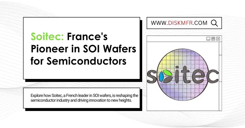
Soitec was founded in 1992
In France, there is a leading company known for its innovations in SOI (Silicon On Insulator) technology. It ranks sixth in the global wafer market with a 6% market share (preceded by Shin-Etsu Chemical, SUMCO, GlobalWafers, Siltronic, and SK Siltronic), and holds a leading position in the niche market of optimized substrates. This company is the French semiconductor manufacturer, Soitec.
Speaking of Soitec’s history, it can be traced back to the 1960s when France began researching semiconductor technology and established several related research institutes, such as the Microelectronics Institute in Grenoble and the CEA-Leti (French Atomic Energy and Alternative Energies Commission – Nanotechnology Research Center). These institutions later became the core of semiconductor technology development in France, with CEA-Leti eventually giving rise to Soitec.
According to information on Soitec’s official website, two engineers from CEA-Leti, Dr. André-Jacques Auberton-Hervé and Jean-Michel Lamure, co-founded Soitec in 1992. Based on their research results from 1991 in the laboratory, they developed a technology called “Smart Cut.” This technology became the core of Soitec, and the company then began large-scale production of SOI wafers.
The core principle of Smart Cut™ is to implant hydrogen ions to create a layer that can be peeled off, and then transfer this thin silicon layer onto an insulator (usually silicon dioxide).
The SOI wafer produced using Smart Cut™ technology is known as “Silicon On Insulator” (SOI) wafer. It consists of three layers: the bottom layer is a standard silicon substrate, the middle layer is an insulating material (typically silicon dioxide), and the top layer is a very thin layer of single-crystal silicon. Due to its structure, which resembles a familiar sandwich, it is also referred to as a sandwich structure.
This technology from Soitec has revolutionized the manufacturing of semiconductor materials. The SOI wafers produced using Smart Cut™ technology not only improve wafer performance but also significantly reduce production costs. As a result, SOI wafers have become an ideal choice for high-performance electronic devices and are widely used in fields such as electronics, communications, and automotive industries.
02
Developed in the late 1990s
With the increasing demand for high-performance, low-power chips in the semiconductor industry, SOI wafers began to gain significant traction. By the late 1990s, Soitec’s customer base expanded rapidly, including major industry giants such as Intel, STMicroelectronics, Sony, and others.
Riding on this momentum, in February 1999, Soitec was listed on the Paris New Stock Exchange (later the Euronext Paris). After going public, the company invested heavily in the creation of the world’s largest SOI production center, Bernin I, to begin producing 200mm and smaller wafers, with an annual production capacity of 800,000 wafers. The following year, Soitec established a second factory, Bernin II, specifically for the production of 300mm wafers, with an annual capacity of 720,000 wafers. It was also in that year that the company’s revenue first surpassed 100 million euros.
In the following years, Soitec continued to expand its overseas market and made two major acquisitions: In 2003, it entered the composite materials production field by acquiring the composite materials technology expert Picogiga International; In 2010, Soitec entered the solar power generation field by acquiring 80% of the shares of Concentrix Solar, a provider of concentrated photovoltaic (CPV) systems.
03
Turning Point 2015
From the above actions, it is clear that Soitec aimed to diversify its business by venturing into fields such as solar energy, LED lighting, and others, in order to reduce its reliance on its core SOI business. The idea was good, but things didn’t go as planned. These new ventures did not bring the expected returns and, instead, increased the company’s operating costs. For example, in the solar photovoltaic sector, Soitec invested heavily with confidence and developed concentrated photovoltaic (CPV) technology. However, the market response to this technology was poor, and the demand did not meet expectations, which led to business losses and a debt crisis for the company.
After going through these struggles, the company finally saw the reality and decided to return to its core business. Under the leadership of then-CEO Paul, Soitec shut down its solar business and refocused on its core SOI business. Looking at the company’s later development, this was clearly the right decision.
As SOI technology gradually matured, Soitec’s position in the global semiconductor materials market steadily rose. Especially in low-power and high-performance applications, SOI wafers became a key material. Soitec gradually expanded globally, setting up multiple production bases and further promoting its SOI technology through collaborations with other semiconductor companies and research institutions.
According to research firm MarketsandMarkets, the global SOI market size is expected to grow from $1.4 billion in 2022 to $2.9 billion in 2027, with a compound annual growth rate (CAGR) of 15.0%. Soitec holds a leading position in the market with around 70% of the global market share. In addition, Japan’s Shin-Etsu Chemical, SUMCO, and the U.S. company GlobalFoundries are also involved, and some domestic manufacturers are gradually emerging in the SOI field.
Although SOI (Silicon-On-Insulator) wafers still account for a relatively small share of the overall wafer market, the future growth of the market is significant, driven by the demands of 5G communications, automotive electronics, and high-performance computing.

Disclaimer:
- This channel does not make any representations or warranties regarding the availability, accuracy, timeliness, effectiveness, or completeness of any information posted. It hereby disclaims any liability or consequences arising from the use of the information.
- This channel is non-commercial and non-profit. The re-posted content does not signify endorsement of its views or responsibility for its authenticity. It does not intend to constitute any other guidance. This channel is not liable for any inaccuracies or errors in the re-posted or published information, directly or indirectly.
- Some data, materials, text, images, etc., used in this channel are sourced from the internet, and all reposts are duly credited to their sources. If you discover any work that infringes on your intellectual property rights or personal legal interests, please contact us, and we will promptly modify or remove it.


