
01
Overview of Electrostatic Chuck (ESC)
The Electrostatic Chuck (ESC) is a clamping device that uses electrostatic force to adsorb a wafer onto a base, and it is widely used in wafer processing technologies under vacuum environments such as plasma etching (Etch) and ion implantation (Implant).
Its core advantages are:
- No physical clamping, avoiding mechanical stress;
- Maintains wafer surface integrity;
- Supports wafer temperature control and high vacuum environments.
02
Working Principle of Electrostatic Chuck
✅ Basic Principle
The basic structure of an electrostatic chuck can be compared to a capacitor:
- The ESC body contains one or more metal electrodes;
- The electrodes are covered with an insulating dielectric layer;
- The wafer, acting as the other pole, is placed on the surface of the dielectric;
- When a voltage is applied to the electrodes, an electric field is formed, inducing opposite charges on the back of the wafer → Electrostatic force fixes the wafer in place.
This force is called Coulomb Force, and as long as the voltage is maintained, the adsorption is sustained.
✅ Simplified Formula for Adsorption Force
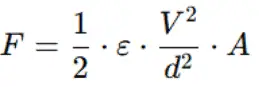
Where:
- F is the electrostatic force,
- ε\varepsilonε is the permittivity of the medium,
- V is the voltage,
- d is the distance between the plates,
- A is the area of the plates.
03
Types of ESC
✅ Unipolar Type
Only one electrode is connected to a voltage; the wafer becomes charged through plasma or other means, forming the counter-electrode.
Simple structure, but requires assistance from a plasma environment;
Commonly used in processes such as etching.
Features:
- Strong chucking force;
- Easily affected by process conditions.
✅ Bipolar Type
Two electrodes are connected to positive and negative voltages respectively, allowing the wafer to be adsorbed without relying on plasma;
More suitable for wafer handling in non-plasma environments.
Features:
- More precise control;
- Adsorption force is 1/4 that of unipolar type under the same voltage (theoretical value);
- Safer and more reliable.
04
ESC Materials and Structural Types
✅ Coulomb Type
Insulator electrode structure;
Requires higher voltage (3000~4000V) to generate sufficient adsorption force;
Simple structure, fast response.
✅ Johnson-Rahbek (JR) Type
Made from doped semiconductor materials (e.g., doped AlN);
Certain conductivity, dense surface charges, small distance between electrodes;
High adsorption force, low required voltage (500~800V);
Suitable for high-temperature, long-duration adsorption.
05
ESC Functional Extensions
In addition to wafer adsorption, modern ESCs typically include:
Backside helium cooling system: maintains uniform wafer temperature;
Temperature-controlled electrodes: improves thermal conduction;
Microstructured patterned surface: optimizes adsorption uniformity and particle release control;
Surface coating technologies: such as PECVD, PVD, polymer coatings, to optimize thermal and electrical performance.
06
Interaction Between ESC and Process
Relationship between plasma self-bias and ESC voltage
Why can’t negative voltage be directly applied under the ESC to enhance plasma self-bias?
The capacitance-resistance model between ESC and wafer causes most DC voltage to concentrate between the ESC and wafer;
The plasma sheath is not controlled by this DC and cannot form an effective self-bias;
Adding DC may instead affect adsorption stability and cause wafer displacement.
Solution:
Introduce low-frequency RF bias (e.g., 400kHz~2MHz) to effectively increase ion energy;
RF bias mainly affects the plasma sheath, truly altering self-bias behavior.
07
Performance Parameter Case Analysis
Assumption:
12-inch wafer, diameter 300mm;
Backside He pressure 20 Torr (approx. 2660 Pa);
Effective ESC adsorption area A ≈ π*(0.15)^2 ≈ 0.07 m²;
Then the pressure on the wafer is:
F=P•A=2660•0.07≈187N
To achieve reliable adsorption force, the ESC voltage and structure must be capable of withstanding this magnitude of force.
08
ESC Design Optimization Directions
To enhance chucking force and process compatibility, key considerations include:
Material Selection:
- High dielectric constant (e.g., Al₂O₃);
- Good thermal conductivity;
- Surface resistance to corrosion and wear.
Structural Design:
- Minimize insulation thickness (balancing breakdown voltage);
- Increase effective contact area;
- Optimize surface microstructures and grooves.
Power Control:
- Precise DC / RF control;
- Fast charge/discharge design for efficient chuck/dechuck;
- Monitor leakage current to prevent wafer damage.
08
Conclusion
Electrostatic chucks are indispensable high-precision components in modern semiconductor micromachining. Through the deep integration of dielectric materials, electrode structures, and process control, they enable non-destructive wafer fixation and efficient thermal management. Understanding their electrical, thermal, and material interaction principles is fundamental to designing and tuning micro/nano fabrication equipment.

Disclaimer:
- This channel does not make any representations or warranties regarding the availability, accuracy, timeliness, effectiveness, or completeness of any information posted. It hereby disclaims any liability or consequences arising from the use of the information.
- This channel is non-commercial and non-profit. The re-posted content does not signify endorsement of its views or responsibility for its authenticity. It does not intend to constitute any other guidance. This channel is not liable for any inaccuracies or errors in the re-posted or published information, directly or indirectly.
- Some data, materials, text, images, etc., used in this channel are sourced from the internet, and all reposts are duly credited to their sources. If you discover any work that infringes on your intellectual property rights or personal legal interests, please contact us, and we will promptly modify or remove it.


