In the intricate and precise manufacturing system of the semiconductor industry, wafer dicing is an indispensable key process responsible for converting large-diameter single-crystal silicon wafers into smaller wafers suitable for chip production. As the final step in semiconductor manufacturing, this process must not only achieve precise dimensional division but also ensure that the surface of the diced wafers meets extremely high standards of flatness and smoothness, thus laying a solid foundation for subsequent chip fabrication. Wafer dicing is one of the back-end processes in advanced packaging, enabling the division of wafers into individual chips for subsequent die bonding, wire bonding, and testing.
Currently, several mainstream wafer dicing techniques in the industry have their respective advantages and are suited to different production requirements:
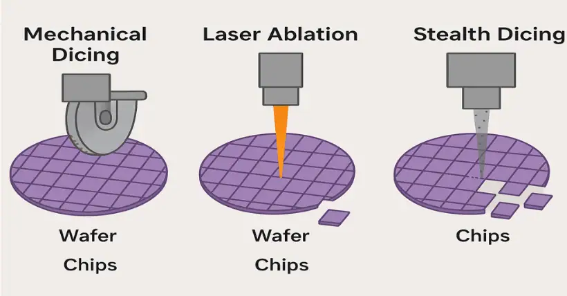
Mechanical Dicing
This is a widely used traditional method in wafer dicing, mainly employing diamond blades or grinding wheels to cut the wafer into target dimensions through high-speed rotation and applied pressure. With its fast cutting speed, it can efficiently meet mass production needs. However, it has evident drawbacks: it tends to produce significant dicing defects and increases surface roughness, negatively impacting subsequent processing precision.
Laser Dicing
As a non-contact dicing technology, laser dicing uses a high-energy laser beam generated by a laser source to process wafers. Thanks to its high precision, low defect rate, and excellent surface quality, it is especially suitable for scenarios with stringent precision and quality requirements in chip manufacturing. However, the high cost of laser equipment and the need for highly skilled operators limit its application in large-scale industrial production. Generally, the process requires that no metal be present in the dicing path.
Hybrid Dicing
This innovative method combines the advantages of mechanical and chemical dicing. It starts with mechanical dicing to preliminarily slice the wafer into thin sheets, followed by chemical solutions for secondary dicing to achieve final dimensioning. This method effectively compensates for the defect-prone nature of mechanical dicing and the low efficiency of chemical dicing, significantly enhancing production efficiency while ensuring dicing precision.
High-Energy Ion Beam Dicing
This technology uses high-energy ion beams to dice wafers, achieving damage-free, high-precision cuts that avoid dicing defects and surface roughness, making it an ideal choice for high-end chip manufacturing. However, due to the complex structure of the equipment and high operational costs, this method is currently mainly used in special production scenarios with extremely high product quality requirements.
After the front-end process is completed and chips are prepared on the wafer, they must be separated through dicing and then packaged. Different wafer thicknesses require different dicing techniques:
- Wafers with a thickness above 100μm generally use blade dicing.
- Wafers thinner than 100μm generally use laser dicing, which reduces chipping and cracking, although efficiency drops significantly above 100μm.
- Wafers thinner than 30μm use plasma dicing, which offers fast speeds and causes no surface damage, thereby improving yield, though the process is more complex.
To ensure dicing quality and production efficiency, the following key factors must be emphasized in the wafer dicing process:
Dicing Speed
This refers to the time required to dice a single wafer and directly impacts production efficiency. While increasing speed boosts capacity, excessive speed can degrade quality, leading to defects and rough surfaces.
Dicing Loss
This refers to the material loss during dicing. Reducing dicing loss not only improves material utilization but also helps control production costs and enhances economic benefits.
Dicing Precision
This refers to the accuracy of wafer dimensions after dicing and directly affects process precision in chip manufacturing. Higher dicing precision reduces production errors and ensures product quality consistency.
Diced Surface Quality
This mainly concerns the flatness and smoothness of the wafer surface after dicing. High surface quality helps minimize disruptions in subsequent processes and supports improved chip performance and yield.
In conclusion, wafer dicing is a critical step in semiconductor manufacturing, with each technique offering unique strengths and limitations. In practice, companies must select the most appropriate dicing method based on specific product requirements, production scale, and budget, taking into account factors such as speed, loss, precision, and surface quality, to ensure the diced wafers meet the stringent demands of chip manufacturing and support the continued advancement of the semiconductor industry.
Related:

Disclaimer:
- This channel does not make any representations or warranties regarding the availability, accuracy, timeliness, effectiveness, or completeness of any information posted. It hereby disclaims any liability or consequences arising from the use of the information.
- This channel is non-commercial and non-profit. The re-posted content does not signify endorsement of its views or responsibility for its authenticity. It does not intend to constitute any other guidance. This channel is not liable for any inaccuracies or errors in the re-posted or published information, directly or indirectly.
- Some data, materials, text, images, etc., used in this channel are sourced from the internet, and all reposts are duly credited to their sources. If you discover any work that infringes on your intellectual property rights or personal legal interests, please contact us, and we will promptly modify or remove it.


