01
What is Chip “Thinning”?
“Thinning,” also known as Back Grinding (BG), is the process of grinding the backside of a wafer down to a target thickness. This step typically occurs after the front-end circuit fabrication of the chip is complete but before the wafer is diced (i.e., while the wafer is still intact). It serves as a bridge between chip fabrication and packaging.
Why is thinning necessary?
After fabrication, wafer thickness is usually quite large (about 700–800 microns). Without thinning:
- It takes up more space during packaging, hindering efforts to make chips thinner and smaller;
- The final packaged chip may not meet the thickness or thermal performance requirements of end products;
- Multi-chip stacking (e.g., 3D packaging) becomes difficult.
Thus, the purpose of thinning is to make chips thinner and more compatible with packaging and system integration requirements.
02
What are The Steps in the Thinning Process?
✅ Coarse Grind
Purpose: Quickly reduce wafer thickness from its original level to near the target thickness, such as from 775μm to 300μm;
Characteristics: Uses coarse grinding wheels for high removal efficiency, but creates a noticeable stress or damage layer on the wafer’s backside;
Risks: Stress accumulation and silicon debris can lead to breakage in subsequent steps.
✅ Fine Grind
Purpose: Further thin the wafer to the final target thickness (e.g., 100–300μm), while removing the damage layer (about 1–2μm) from coarse grinding;
Tools: Uses grinding wheels with smaller grain sizes and higher precision;
Key points: Ensure surface flatness and minimize new damage
✅ Cleaning
Essential step: Coarse and fine grinding generate a large amount of silicon debris. If not removed promptly, it may remain on the wafer surface or edges;
Materials: High-purity water (DI water) + surfactants to remove residues and prevent contamination or chip damage during packaging;
Goal: Ensure wafer cleanliness and improve downstream yield.
03
Challenges and Key Control Points in Thinning
✅ Wafer Breakage Risk
Thinner wafers are more brittle and fragile;
It is crucial to control grinding uniformity, pressure, temperature, and equipment flatness to avoid generating “micro-cracks.”
✅ Wafer Warpage
Post-thinning, wafers may warp due to uneven stress, affecting lamination, dicing, and packaging;
Process optimization is needed for back support or temporary bonding materials.
✅ Yield Control
If micro-cracks caused by grinding are not completely removed, the chips may break during dicing or assembly, reducing yield.
04
Post-Thinning Actions
After thinning:
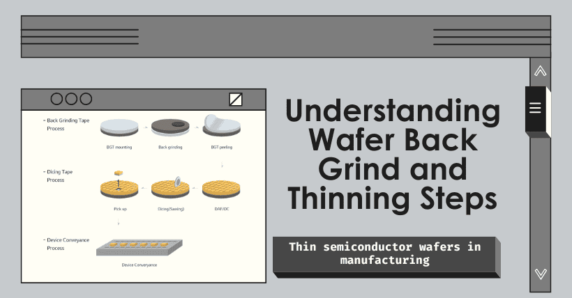
- The wafer is usually laminated with Back Grinding Tape for protection;
- Then it enters the dicing stage, where it’s cut into individual chips;
- Afterward, it proceeds to packaging (e.g., BGA, QFN, WLCSP, etc.).
05
Example
Take a mobile SoC chip as an example:
- The design requires a thickness of less than 0.3mm;
- After circuit completion, wafer thickness is about 775μm;
- Coarse grinding reduces it to 350μm, and fine grinding further thins it to 280μm;
- After cleaning, the wafer proceeds to dicing and packaging.
06
Summary
Thinning in packaging is not just a simple material removal step, but a complex process involving mechanics, materials science, and thermodynamics. Its success directly impacts the mechanical stability, reliability, and dimensional design of the final chip. A high-quality thinning process is the foundation for achieving high yield and high reliability in advanced chip packaging.

Disclaimer:
- This channel does not make any representations or warranties regarding the availability, accuracy, timeliness, effectiveness, or completeness of any information posted. It hereby disclaims any liability or consequences arising from the use of the information.
- This channel is non-commercial and non-profit. The re-posted content does not signify endorsement of its views or responsibility for its authenticity. It does not intend to constitute any other guidance. This channel is not liable for any inaccuracies or errors in the re-posted or published information, directly or indirectly.
- Some data, materials, text, images, etc., used in this channel are sourced from the internet, and all reposts are duly credited to their sources. If you discover any work that infringes on your intellectual property rights or personal legal interests, please contact us, and we will promptly modify or remove it.


