01
What is Wafer Sawing?
Wafer sawing refers to the process of cutting hundreds or thousands of chips (dies) that have been fabricated on a single wafer into individual die units along predefined scribe lines.
In simple terms, it’s like precisely cutting a large “cake” into small pieces to facilitate subsequent individual packaging.
02
Purpose and Significance of Wafer Sawing
Why do we need wafer sawing?
Chip separation: A wafer is initially a whole piece, but each chip must be individually packaged and tested, requiring separation.
Facilitates packaging: Each chip needs to be individually handled, electrically tested, and packaged, which must be achieved through sawing.
Improves yield and reliability: A finely controlled sawing process can reduce edge chipping and increase the success rate of final packaging.
03
Key Technical Parameters of Wafer Sawing
Sawing is not simply “cutting”; it’s a precise process. Key parameters include:
| Parameter | Description |
|---|---|
| Blade speed | Typically 50 mm/s; too fast may damage chips, too slow affects efficiency. |
| Spindle speed | Generally 38,000 rpm; needs adjustment based on blade material and chip hardness. |
| Cut width | Standard blades cut ~40 microns; laser cutting can reduce to 20 microns. |
| Water quality | Resistivity below 1 MΩ·cm to avoid electrostatic damage. |
| Water spray angle/flow | Precisely controlled to prevent tool overheating and wash away silicon debris. |
04
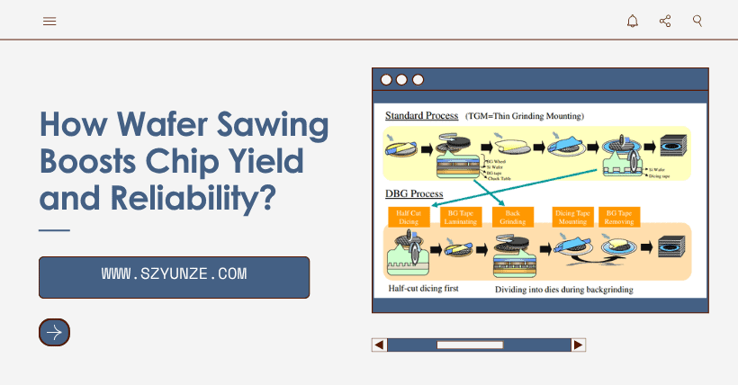
Standard Wafer Sawing Process (Step by Step)
Step 1: Blue tape mounting
The wafer is fixed onto blue tape, which is mounted on a metal frame, ready for sawing.
Step 2: Scribe path setting
The sawing equipment sets the cut path based on chip layout, ensuring cuts are along scribe lines without damaging chip areas.
Step 3: Blade or laser selection
- Standard chips use regular blades
- High-precision, narrow-pitch, stacked chips use laser sawing
Step 4: Cutting operation
- The blade starts rotating and moves slowly along the set path
- Ultra-pure water is sprayed to remove cutting dust and cool the tool
- Each wafer requires tens to hundreds of cuts
Step 5: Prevent blue tape penetration
Cutting depth must be precisely controlled. If the blue tape is penetrated, chips will scatter and cannot proceed to packaging.
05
Special Wawing Techniques
Laser cutting
Used for ultra-small chips, ultra-narrow cutting lanes, or 3D stacked packages
Advantages: no mechanical stress, high precision, narrow cut width
Dual-blade sawing
Some chips require two-stage cutting to protect the surface layer:
- First, a wide blade removes the surface protective layer
- Second, a narrow blade performs precise cutting
06
Wafer Wawing Risks and Control Points
| Problem | Cause | Result | Countermeasure |
|---|---|---|---|
| Chip chipping | Improper blade speed/feed | Yield reduction | Optimize blade parameters |
| Silicon debris buildup | Insufficient rinsing water | Contamination, tool wear | Increase water flow and adjust spray angle |
| Electrostatic damage | High water resistivity | Chip failure | Ensure pure water resistivity <1 MΩ |
| Blue tape cut-through | Depth control failure | Chips fall off | Precisely set Z-axis cutting depth |
07
Post-Sawing Cleaning Process
- Clean chip surfaces
- Rinse off residual silicon powder and particles after sawing
- Ensure bond pad area is free of contamination
Additives in water
- Sometimes chemical cleaning agents or CO₂ bubbles are added to pure water to improve cleaning effectiveness and avoid residue interfering with later packaging.
08
Summary
Wafer sawing is the critical step of precisely separating hundreds or thousands of chips on a wafer into individual units. It’s one of the key nodes in yield control.
| Item | Content |
|---|---|
| Definition | The process of cutting a wafer into single chips |
| Process type | Mechanical blade sawing or laser cutting |
| Control factors | Blade speed, spindle speed, water flow, resistivity, depth |
| Cleaning | Pure water rinse, optional chemical additives |
| Risk points | Chipping, static electricity, blue tape cut-through |

Disclaimer:
- This channel does not make any representations or warranties regarding the availability, accuracy, timeliness, effectiveness, or completeness of any information posted. It hereby disclaims any liability or consequences arising from the use of the information.
- This channel is non-commercial and non-profit. The re-posted content does not signify endorsement of its views or responsibility for its authenticity. It does not intend to constitute any other guidance. This channel is not liable for any inaccuracies or errors in the re-posted or published information, directly or indirectly.
- Some data, materials, text, images, etc., used in this channel are sourced from the internet, and all reposts are duly credited to their sources. If you discover any work that infringes on your intellectual property rights or personal legal interests, please contact us, and we will promptly modify or remove it.


