01
What is Wire Bonding?
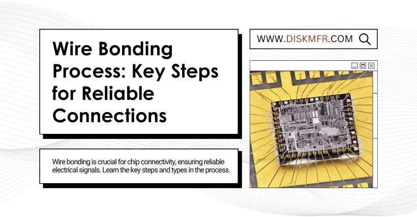
Wire bonding is a key step in “bringing out” the electrical signals from inside the chip. We use extremely thin metal wires (mostly gold, aluminum, or copper) to create electrical connections between the chip’s bond pads and the framework (such as a lead frame or substrate).
It can be understood as:
“The chip is the brain, but it relies on the blood vessels (wires) to transmit signals; otherwise, no matter how smart it is, it can’t do anything.”
02
The Core Purpose of Wire Bonding
Establish electrical connections: Signal channels between the chip’s internal and external packaging.
Ensure reliability: Meet electrical performance and mechanical stability requirements.
Ensure production yield: Lay a good foundation for subsequent packaging.
03
Type of Wire Bonding
Although there are various methods (such as thermocompression bonding, ultrasonic bonding, thermosonic bonding, etc.), the most common type is ball bonding using thermosonic gold wires, which is particularly suitable for the combination of aluminum bond pads and gold wires.
04
The Complete 9-step Process of Wire Bonding (explained step by step)
✅ Step 1: Prepare the gold wire
The gold wire is drawn from the wire bonding machine’s spool and passes through the bottom of the capillary, exposing a short tail of wire.
✅ Step 2: Form the “free air ball” (FAB)
The wire bonding machine uses a “discharge” method to form a gold ball at the tail of the gold wire. This ball is naturally formed in the air, hence called a free air ball.
It’s like using an electric spark to melt the wire’s end, forming a gold bead.
✅ Step 3: Press the ball onto the chip’s bond pad
The capillary with the gold ball aligns with the bond pad on the chip, then gently presses down to make the ball adhere to the pad.
✅ Step 4: Complete the first bond (ball bond)
After pressing, the wire bonding machine applies:
A certain amount of pressure
A specific amount of ultrasonic energy
Control over the bonding time
The purpose is to cause plastic deformation and micro-friction welding between the gold ball and the chip’s bond pad, securely bonding them together.
✅ Step 5: Pull the gold wire
The capillary lifts, pulling the gold wire and creating an arc-shaped line starting from the chip’s bond pad, extending to the target point: the bond pad on the framework (lead/frame pad or PCB pad).
✅ Step 6: Press the wire onto the frame’s bond pad
The capillary moves to the position of the frame’s bond pad and presses the wire down again.
✅ Step 7: Form the second bond (tail bond)
Pressure, ultrasonic energy, and time control are applied once more. This time, instead of pressing a ball, the gold wire is pressed into a “fish tail” shape, attaching it to the frame’s bond pad, completing the second welding.
✅ Step 8: Cut the wire and leave the tail
The capillary continues to lift and cuts the gold wire, leaving the “fish tail” on the frame’s bond pad, while leaving a new wire tail at the capillary’s tip, preparing for the next wire.
✅ Step 9: Cycle through to bond the next wire
Return to Step 1 and repeat the process until all bond pads are connected.
05
The Four Core Parameters of the Wire Bonding Process
| Parameter | Function | Example Explanation |
|---|---|---|
| Temperature (Bond Temp) | Increases metal plasticity, improves welding effect | Usually 100~150°C |
| Pressure (Bond Force) | Ensures sufficient contact and deformation | Too small will not weld firmly, too large will damage the pad |
| Ultrasonic Power | Triggers friction/diffusion between metal molecules | Control the energy to avoid “cold welds” or “flying wires” |
| Ultrasonic Time (Bond Time) | Determines the duration of ultrasonic action | Used in conjunction with energy, should not be too short or too long |
06
Key Control Points for Bonding Quality
1️⃣ Gold ball size control:
Gold ball diameter: typically 60μm
Thickness: approximately 20μm
Too large may cause short circuits, too small may result in weak bonding
2️⃣ Bond strength testing:
Shear/Push Force: The push force on the chip-side gold ball should be > 20g
Pull Force: The wire should withstand > 109g before breaking
These tests are standard procedures to verify whether the bond strength meets the requirements and should not be overlooked.
07
Environmental and Process Considerations
⚠️ 1. Moisture control:
If wire bonding is delayed for more than 72 hours, low-temperature baking is required to remove absorbed moisture.
Otherwise, during the molding process, water vapor may expand, causing cracks in the package or delamination of the interface.
⚠️ 2. Surface cleanliness:
If the bond pad is contaminated or has an oxide layer, it will directly cause bonding failure (gold ball detachment or poor fish tail adhesion).
If necessary, a plasma cleaner can be used for surface activation to restore weldability.
08
What are the Reliability Risks after Wire Bonding?
| Issue Phenomenon | Possible Cause | Solution |
|---|---|---|
| Gold ball detachment | Pad oxidation, low temperature, insufficient ultrasound | Clean the surface, adjust parameters |
| Gold wire breakage | Damaged gold wire, excessive curvature | Optimize wire pulling path, change wire material |
| Fish tail lift | Insufficient pressure, bracket oxidation | Apply more pressure, clean the bracket surface |
| High contact resistance | Insufficient solder joint, weak welding | Adjust ball size, ultrasonic energy |
09
Wire bonding in the entire packaging process
Wafer cutting → 2. Chip mounting → 3. Silver paste baking →Wire bonding → 5. Molding → 6. Electrical testing → 7. Final sorting
10
Summary
Wire bonding is one of the most detailed and crucial steps in chip packaging, involving mechanical precision, material properties, and the control of thermal/ultrasonic parameters. Although the gold wire is as thin as a hair, it carries the important task of connecting the chip to the external world.
In simple terms: “The gold wire is as fine as a thread; a single mistake can ruin an entire batch.”
Related:

Disclaimer:
- This channel does not make any representations or warranties regarding the availability, accuracy, timeliness, effectiveness, or completeness of any information posted. It hereby disclaims any liability or consequences arising from the use of the information.
- This channel is non-commercial and non-profit. The re-posted content does not signify endorsement of its views or responsibility for its authenticity. It does not intend to constitute any other guidance. This channel is not liable for any inaccuracies or errors in the re-posted or published information, directly or indirectly.
- Some data, materials, text, images, etc., used in this channel are sourced from the internet, and all reposts are duly credited to their sources. If you discover any work that infringes on your intellectual property rights or personal legal interests, please contact us, and we will promptly modify or remove it.


