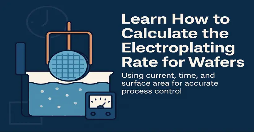
Friends often ask how the electroplating rate is calculated. Many people have always been unclear and rely on experience values for wafer electroplating rates.
For divalent metals like copper, under the condition of 1 ASD and 1 minute, the growth is about 0.2 μm.
What is ASD?
ASD = A/dm² = amperes per square decimeter, i.e., the unit of current density. It represents the current intensity applied per unit area. Deposition rate, crystal quality, stress, and uniformity are all directly affected by current density.
Deriving wafer electroplating speed using Faraday’s First Law:
Faraday’s research shows that in the electroplating process, the amount of substance reduced and deposited on the cathode is proportional to the current intensity and the duration of current flow.
The formula is:
m = KQ = KIt
Where:
m — mass of metal deposited
K — proportional constant
Q — total electric charge
I — current intensity
t — duration of current
Also, Q = nZF, where:
n = moles of product [mol]
Q = total electric charge [C]
z = valency
F = 96485.33212…
Thus:
It = m / (M·Z·F)
and m = ρ·s·h, I = D·s
s = electroplating area
h = electroplating thickness
D = current density
M = molar mass
ρ = metal density (ρ_copper = 8.92 g/cm³ = 8920 g/dm³)
Substituting:
D·s·t = (ρ·s·h) / (M·Z·F)
Dt = h·M / (ρ·Z·F)
h = DtM / (ρ·Z·F) = DtM / (8920·2·96485)
If D = 1 ASD, t = 1 min = 60 s, M = 63.5:
h = 1×60×63.5 / 19297000 = 0.00000227 dm = 0.227 μm
Considering current efficiency, our experience value for copper plating is around 0.2 μm. For other metals, the plating rate can be deduced accordingly.
Related:

Disclaimer:
- This channel does not make any representations or warranties regarding the availability, accuracy, timeliness, effectiveness, or completeness of any information posted. It hereby disclaims any liability or consequences arising from the use of the information.
- This channel is non-commercial and non-profit. The re-posted content does not signify endorsement of its views or responsibility for its authenticity. It does not intend to constitute any other guidance. This channel is not liable for any inaccuracies or errors in the re-posted or published information, directly or indirectly.
- Some data, materials, text, images, etc., used in this channel are sourced from the internet, and all reposts are duly credited to their sources. If you discover any work that infringes on your intellectual property rights or personal legal interests, please contact us, and we will promptly modify or remove it.


