Gate-Induced Drain Leakage (GIDL) in MOSFETs refers to a leakage current phenomenon occurring in the channel region under the gate dielectric when the gate voltage is relatively high. This effect is caused by a high electric field inducing electron tunneling through the dielectric layer, forming a leakage current. GIDL current has become one of the main factors affecting the reliability and power consumption of small-sized MOS devices, and it also significantly impacts the erase/write operations of memory devices. As semiconductor technology enters the ultra-deep submicron era and device dimensions shrink, the reliability issues caused by GIDL current become more severe. As MOSFETs are core components of integrated circuits, understanding their characteristics is crucial in the ongoing advancement toward smaller, higher-performance semiconductor devices.
01
Physical Origin of GIDL Effect
The essence of the GIDL effect lies in the quantum mechanical tunneling phenomenon. When there is a large voltage difference between the gate and drain of a MOSFET, a strong electric field is generated beneath the gate. Under this electric field, the energy bands near the drain region of the semiconductor bend significantly, bringing the valence and conduction bands closer in space, which are normally separated by the bandgap. Electrons in the valence band can then tunnel directly into the conduction band via quantum tunneling, without requiring thermal excitation, resulting in an additional drain leakage current—i.e., GIDL current. This quantum-effect-based current generation mechanism is fundamentally different from traditional thermally activated conduction and is an unavoidable phenomenon in nanoscale MOSFETs.
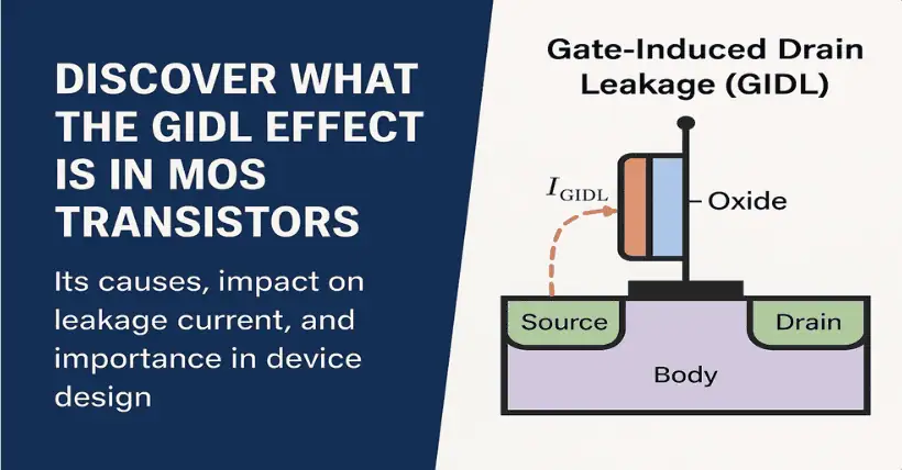
In MOSFETs, the leakage currents contributing to static power dissipation mainly include subthreshold leakage from source to drain, gate leakage current, and gate-induced drain leakage (GIDL) occurring in the gate-drain overlap region, as shown in the figure. Among these, when the device is in the off state or in standby, GIDL current dominates the total leakage. GIDL occurs in the gate-drain overlap region, which is a critical area in the MOSFET. The typical GIDL testing structure is a gated-diode (GD) configuration, where the device is in the off state during testing. When the gate-drain voltage (VG) is high at the gate-drain overlap, electrons in the silicon near the overlap interface undergo band-to-band tunneling from the valence to conduction band, forming what is known as GIDL tunneling current. As the gate oxide layer becomes thinner, GIDL tunneling current increases sharply.
02
Key Factors Affecting GIDL Effect
The intensity of the GIDL effect is not fixed and is influenced by various device parameters and operating conditions. From a structural perspective, gate oxide thickness is a crucial factor. A thinner oxide layer strengthens the gate electric field and increases the degree of band bending, thereby significantly enhancing GIDL current. Substrate doping concentration also plays an important role—higher doping levels alter the semiconductor band structure, making band bending more likely, thus intensifying the GIDL effect. In terms of operating conditions, increasing the drain voltage directly raises the electric field between the gate and drain, facilitating electron tunneling and significantly increasing GIDL current.
03
Multiple Challenges Brought by GIDL Effect
GIDL effect poses numerous challenges in the design and application of integrated circuits. From a power perspective, GIDL current contributes to additional static power consumption, which is particularly critical in low-voltage, low-power chip designs, significantly reducing battery life and limiting product usage time. In terms of performance, GIDL effect can cause drift in the MOSFET threshold voltage, affecting switching behavior and potentially leading to logic errors in circuits, even complete chip failure in severe cases. From a reliability standpoint, persistent GIDL current accelerates device aging, shortens chip lifespan, and increases maintenance costs and failure risks.
04
Effective Strategies to Suppress GIDL Effect
To address the challenges posed by GIDL, the industry has adopted strategies from both device structure optimization and circuit design. On the device side, replacing traditional silicon dioxide with high-k dielectric materials helps maintain gate capacitance while allowing a thicker gate dielectric, effectively weakening the gate electric field. Adjusting substrate doping profiles to reduce doping concentration near the drain can decrease band bending, suppressing GIDL current. On the circuit design side, properly setting bias voltages to avoid excessive gate-drain voltage differences can reduce GIDL at the source, while employing advanced circuit architectures and design techniques can enhance the circuit’s immunity to the GIDL effect.

Disclaimer:
- This channel does not make any representations or warranties regarding the availability, accuracy, timeliness, effectiveness, or completeness of any information posted. It hereby disclaims any liability or consequences arising from the use of the information.
- This channel is non-commercial and non-profit. The re-posted content does not signify endorsement of its views or responsibility for its authenticity. It does not intend to constitute any other guidance. This channel is not liable for any inaccuracies or errors in the re-posted or published information, directly or indirectly.
- Some data, materials, text, images, etc., used in this channel are sourced from the internet, and all reposts are duly credited to their sources. If you discover any work that infringes on your intellectual property rights or personal legal interests, please contact us, and we will promptly modify or remove it.


