The wafer electroplating rate cannot be increased indefinitely because semiconductor processes generally follow the principle of “more haste, less speed.” To achieve high quality, the process must be slowed down.
How to increase the wafer electroplating rate?
Fundamental mechanism: The plating rate can only be increased by raising the product of cathode (wafer) current density and current efficiency. Therefore, efforts must focus on improving both current density and current efficiency.
Problems encountered when increasing current density:
- When current density increases sharply, current efficiency decreases, and side reactions (such as hydrogen evolution) intensify. Increased hydrogen evolution can cause pinholes and other defects.
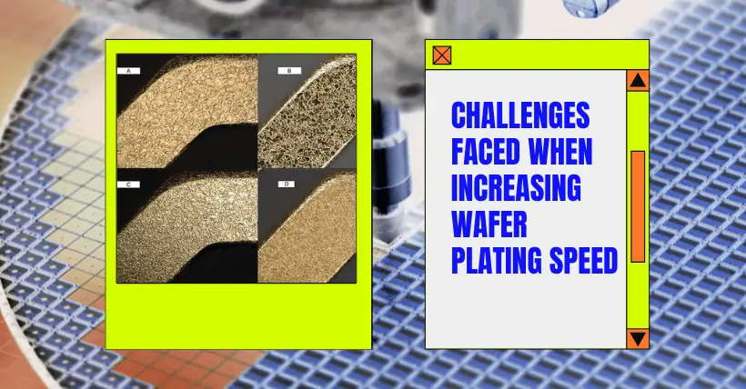
- When cathode current density is too high, the energy of deposited atoms increases. Crystals grow not only laterally on the surface but also vertically or in three-dimensional space, easily leading to dendritic or rough coatings.
- Levelers and brighteners can effectively control crystal morphology at low speeds, but at high current density, additives either diffuse too slowly or are rapidly reduced and consumed. This weakens surface leveling capability; brighteners become ineffective, resulting in grainy surfaces or areas with poor brightness.
How to eliminate problems caused by increased current density?
- Enhance electrochemical polarization: use additives that can withstand higher current densities; increase plating bath temperature; roughen the surface, etc.
- Reduce concentration polarization: enhance solution movement (stirring/spraying/rotating cathode/air bubbling); increase plating solution concentration. The next topic will cover what electrochemical polarization and concentration polarization are.
Related:
- How Polarization Impacts Wafer Electroplating Process?
- Wafer Electroplating: Key Laws You Must Follow Now

Disclaimer:
- This channel does not make any representations or warranties regarding the availability, accuracy, timeliness, effectiveness, or completeness of any information posted. It hereby disclaims any liability or consequences arising from the use of the information.
- This channel is non-commercial and non-profit. The re-posted content does not signify endorsement of its views or responsibility for its authenticity. It does not intend to constitute any other guidance. This channel is not liable for any inaccuracies or errors in the re-posted or published information, directly or indirectly.
- Some data, materials, text, images, etc., used in this channel are sourced from the internet, and all reposts are duly credited to their sources. If you discover any work that infringes on your intellectual property rights or personal legal interests, please contact us, and we will promptly modify or remove it.


