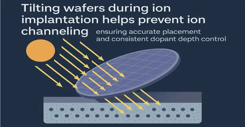
In the semiconductor manufacturing process, tilting the wafer at a certain angle (typically 5° to 7°) during ion implantation is a key process adjustment. The primary purpose is to mitigate the adverse effects of the channeling effect and ensure the accuracy and uniformity of ion implantation. The specific reasons and principles are as follows:
I. Hazards of the Channeling Effect
- What is the Channeling Effect?
Semiconductor materials (such as monocrystalline silicon) have a crystal structure with periodic atomic arrangements, forming regular atomic “channels.”
When ions are implanted in a direction parallel to the crystal orientation (such as <100> or <111>), they may penetrate deep into the wafer along the atomic channels, resulting in:
- Implantation depth far greater than expected (several to dozens of times deeper than the normal range).
- Uneven concentration distribution (locally excessive or insufficient dosage).
- Impact on Device Performance
The channeling effect can cause threshold voltage shifts in transistors, increased leakage current, or parameter inconsistencies, seriously affecting chip yield and performance.
II. Principle of Using Tilt Angles to Suppress Channeling
- Disrupting Ion Parallelism with the Crystal Orientation
By tilting the wafer 5° to 7° (often combined with rotation, e.g., 30° rotation around the normal), the ion implantation direction deviates from the major crystal orientations.
Ions no longer travel straight along atomic channels but undergo multiple scattering collisions with atoms, gradually losing energy and ultimately stopping within the intended depth range.
- Effectively Increasing the Scattering Probability
The tilt angle increases the angle between the ion path and the crystal atomic rows, significantly enhancing the collision probability, thereby:
- Shortening the effective range, allowing the concentration peak to meet design requirements.
- Equalizing the depth distribution to avoid localized over-deep or over-shallow anomalies.
III. Other Supporting Measures
Besides tilt angles, the semiconductor process often incorporates the following methods to further suppress the channeling effect:
- Pre-amorphization Implant (PAI)
Inert ions (e.g., Ge) with low energy are implanted first to form an amorphous layer on the wafer surface, destroying the crystal structure and blocking subsequent ion channeling paths.
- Use of Masking Oxide Layers
A layer of silicon dioxide (SiO₂) or silicon nitride (Si₃N₄) is grown in the implantation area. The difference in atomic number between the mask material and silicon increases ion scattering, indirectly suppressing the channeling effect.
IV. Balanced Considerations in Angle Selection
- Risks of Excessive Tilt Angles
If the tilt angle is too large (e.g., more than 10°), it may cause:
- Edge Dose Deviation: The ion incident angle changes more significantly at the wafer edges, worsening dose uniformity. If PR (photoresist) is present during implantation, a large angle may cause shadowing near the PR edge, leading to performance differences due to low-dose areas.
- Equipment Compatibility Issues: Some implant machines require higher mechanical stability for large tilt angles, increasing process complexity.
- Adaptation to Crystal Orientation and Material
Wafers with different crystal orientations (such as <100> or <111>) vary in sensitivity to the channeling effect, requiring experimental optimization of the tilt angle to balance suppression effectiveness and process stability.
Conclusion
The tilt angle during ion implantation is a core technique in semiconductor processes to counteract the channeling effect. By physically disrupting the parallel alignment of ions and the crystal, it enables precise control of implantation depth and concentration. This minor adjustment (just a few degrees) reflects the “atomic-level precision” required in semiconductor manufacturing and is one of the key technologies ensuring the performance of advanced process devices.

Disclaimer:
- This channel does not make any representations or warranties regarding the availability, accuracy, timeliness, effectiveness, or completeness of any information posted. It hereby disclaims any liability or consequences arising from the use of the information.
- This channel is non-commercial and non-profit. The re-posted content does not signify endorsement of its views or responsibility for its authenticity. It does not intend to constitute any other guidance. This channel is not liable for any inaccuracies or errors in the re-posted or published information, directly or indirectly.
- Some data, materials, text, images, etc., used in this channel are sourced from the internet, and all reposts are duly credited to their sources. If you discover any work that infringes on your intellectual property rights or personal legal interests, please contact us, and we will promptly modify or remove it.


