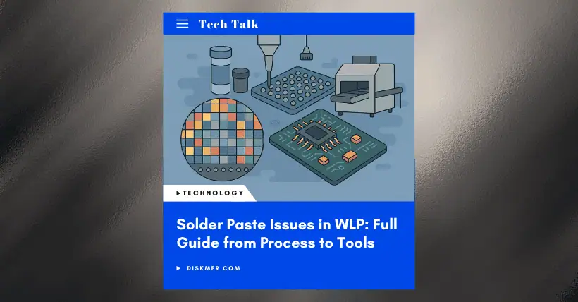
In the precision process of wafer-level packaging, solder paste serves as a core interconnection material, and even minor negligence can trigger a series of issues. From printing to reflow, from equipment parameters to process details, every step carries hidden challenges. Today, engineers at Aoniu Technology analyze these “stumbling blocks” from the perspective of a packaging solder material manufacturer, explore the root causes, and offer key countermeasures.
01
Printing Stage: “Out-of-Control” Risk in Fine Pitch Scenarios
The ultra-fine pitch (≤0.15mm) of wafer-level packaging imposes extreme demands on solder paste printing, with common issues centered around three areas:
Bridging and Short Circuits
When stencil aperture spacing is too small (<50μm), insufficient thixotropy of the solder paste can lead to collapse due to gravity after printing, resulting in bridging.
Insufficient Solder and Incomplete Prints
Excessive roughness (>0.2μm) on the inner wall of electroformed stencil apertures can cause incomplete release of solder paste, forming “crescent defects” at pad edges. On RDL pads in fan-out packages, insufficient solder directly affects the reliability of subsequent ball placement.
Solder Paste Misalignment
Fluctuations in squeegee pressure (>±0.1N) or wafer positioning errors (>3μm) can cause solder paste to shift from the center of the pad, potentially leading to bonding failure during flip chip bump formation.
Process Key Points:
- Stencil Selection: For ultra-fine pitch, prioritize electroformed stencils (aperture tolerance ±1μm) with nano-coating to reduce surface energy.
- Solder Paste Properties: Thixotropic index should be controlled between 5–4.5 (tested via rotational viscometer) to ensure shape stability after printing.
- Equipment Calibration: Calibrate printer X/Y alignment accuracy daily, maintaining error within ±2μm.
02
Reflow Soldering Stage: “Hidden Defects” at High Temperatures
Reflow soldering is a key step in forming solder joints from paste, and high-temperature environments can exacerbate hidden issues:
Excessive Voids
When flux volatilization rate mismatches the ramp profile, voids form inside solder joints. In vertical interconnects of TSV packaging, a void rate exceeding 5% can lead to signal transmission degradation.
Solder Joint Segregation
With SAC system solder pastes, overly fast cooling (>10℃/s) can cause Ag/Cu-rich phase segregation, reducing solder joint fatigue resistance by 40% and failing 1000-cycle automotive thermal cycling tests.
Solder Ball Spattering
Fluctuating oxygen content (>50ppm) in wafer-level reflow ovens can cause solder paste oxidation, leading to spattering at peak reflow temperatures (240–260℃), contaminating adjacent pads.
Process Key Points:
- Ramp Profile: Use a “three-stage” profile (preheat 80–120℃ → soak 150–180℃ → peak 240℃), controlling flux volatilization time within 60–90 seconds.
- Environment Control: Maintain oxygen content at 10–30ppm; nitrogen flow rate at 50–100L/min.
- Cooling Rate: Set a gradual cooling zone at 5–8℃/s to reduce alloy phase segregation.
03
Equipment Matching: Dual Challenge of Precision and Stability
Proper equipment alignment and precision are critical — even the best solder paste underperforms without proper equipment support.
- Squeegee Wear in Printers: When polyurethane squeegee edge wear exceeds 0.5mm, solder paste printing thickness deviates by >±10%, directly affecting bump height consistency in fan-in packaging.
- Temperature Imbalance in Reflow Ovens: If adjacent zones in a multi-zone reflow oven differ by >5℃, solder joint melt depth variation across the wafer can reach 20%, especially on large wafers (≥8 inches).
- Incomplete Stencil Cleaning: Laser cleaning machines with insufficient power (<50W) leave solder paste residue in stencil apertures, causing “secondary contamination” and batch printing defects.
Equipment Key Points:
- Printer: Equipped with automatic squeegee wear detection system; calibrate printing thickness every 50 wafers.
- Reflow Oven: Use infrared + hot air hybrid heating to ensure surface temperature uniformity within ±2℃.
- Stencil Maintenance: Daily cleaning using 100W laser cleaner combined with ultrasonic isopropyl alcohol cleaning to ensure 100% aperture light transmission.
04
Solutions: Collaboration of Materials and Process
To address these challenges, Aoniu Technology has developed specialized solder paste for wafer-level packaging, with three core innovations:
- Enhanced Thixotropy Formula: Added nano-scale fumed silica increases thixotropic index to 4.2, reducing bridging rate to below 0.5% in 0.1mm pitch printing.
- Low-Voiding Flux System: Using modified rosin and organic acid blend, fully volatilized at 240℃ peak temperature, keeping void rate under 3%. Recently, a joint development with a Japanese materials tech company introduced a void suppression agent, significantly reducing voids and improving soldering reliability.
- Wide Temperature Adaptability: Alloy powder sphericity >95%, maintaining solder joint strength (shear force ≥30MPa) even with ±5℃ reflow temperature variation.
The application of solder paste in wafer-level packaging is essentially a “triangle balance” between materials, processes, and equipment. Controlling every parameter in detail ensures that solder paste becomes a true “booster” for improved packaging yield.

Disclaimer:
- This channel does not make any representations or warranties regarding the availability, accuracy, timeliness, effectiveness, or completeness of any information posted. It hereby disclaims any liability or consequences arising from the use of the information.
- This channel is non-commercial and non-profit. The re-posted content does not signify endorsement of its views or responsibility for its authenticity. It does not intend to constitute any other guidance. This channel is not liable for any inaccuracies or errors in the re-posted or published information, directly or indirectly.
- Some data, materials, text, images, etc., used in this channel are sourced from the internet, and all reposts are duly credited to their sources. If you discover any work that infringes on your intellectual property rights or personal legal interests, please contact us, and we will promptly modify or remove it.


