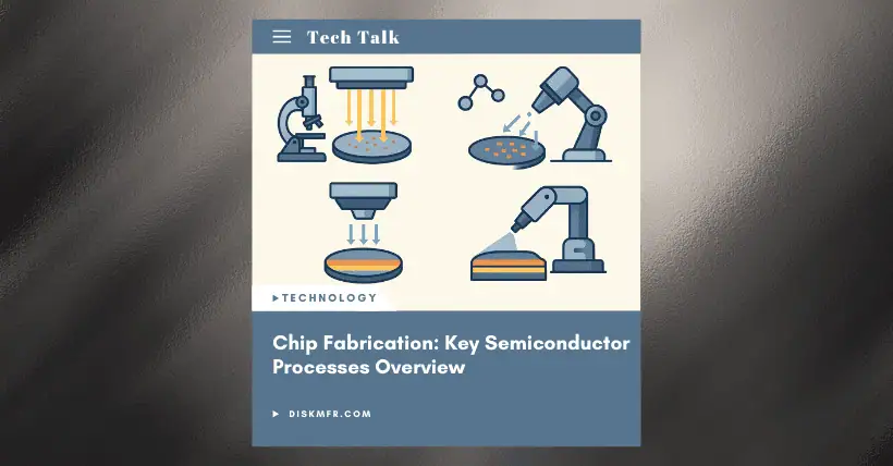
This article introduces several chip fabrication processes. In a Fab, there are four common types of processing technologies: patterning technology (lithography), doping technology, film deposition technology, and etching technology.
Specific processes include lithography, ion implantation, rapid thermal process (RTP), plasma enhanced chemical vapor deposition (PECVD), sputtering, dry etching, and wet etching.
01
Patterning Technology (Lithography)
Patterning technology generally refers to lithography, which is one of the key drivers of the rapid development of semiconductor technology. It originated from photographic plate-making in printing technology.
Lithography allows for any pattern to be defined in micro- and nanoscale using photoresist and then transferred onto materials through combination with other process technologies, realizing various semiconductor material and device designs and ideas.
The light source used in lithography directly affects pattern precision. Common light sources include ultraviolet (UV), deep ultraviolet (DUV), X-rays, and electron beams, with increasing precision in that order.
A standard lithography process includes surface treatment, spin coating, prebake, exposure, post-exposure bake, development, hard bake, and inspection.
The substrate surface usually adsorbs H₂O molecules from the air, which is unfavorable for lithography. Therefore, dehydration baking is required first. For hydrophilic substrates, the adhesion with hydrophobic photoresist is insufficient, which may cause delamination or pattern shifting, hence an adhesion promoter is applied.
Common adhesion promoters include hexamethyldisilazane (HMDS) and trimethylsilyldiethylamine (TMSDEA).
After surface treatment, photoresist is spin-coated. The resist thickness depends not only on its viscosity but also on the spin speed. Roughly, thickness is inversely proportional to the square root of spin speed.
After spin coating, prebaking is done to evaporate solvents in the resist, improving adhesion.
Next is exposure. Photoresists can be positive or negative, with opposite behavior after exposure.
For example, unexposed positive resist is insoluble in developer, while exposed areas become soluble. During exposure, light passes through a patterned mask onto the resist-coated substrate, defining the resist pattern.
Before exposure, alignment between the substrate and mask is crucial for precise positioning. Exposure time must be controlled; too long or too short can distort patterns.
Post-exposure bake is sometimes done to eliminate standing wave effects but is optional and can be skipped before development.
Development dissolves the exposed resist, transferring the mask pattern onto the resist. Development time must be tightly controlled to avoid under- or over-development.
Hard bake strengthens adhesion and enhances etch resistance by further baking the photoresist at a slightly higher temperature than prebake. Finally, pattern inspection is done under a microscope.
After transferring the pattern to material via other processes, the photoresist is removed using either wet or dry stripping. Wet stripping uses strong organic solvents (typically acetone) to dissolve the resist; dry stripping uses oxygen plasma to etch it away.
02
Doping Technology
Doping is also essential in semiconductor technology to alter the electrical properties of semiconductor materials. Two common doping methods are thermal diffusion and ion implantation.
The industry commonly uses ion implantation, involving ion implantation and RTP processes.
(1) Ion Implantation
Ion implantation bombards the substrate with high-energy ions for doping. Compared with thermal diffusion, ion implantation has many advantages. Ions are selected via mass analyzers, ensuring high purity. Substrates remain at room temperature or slightly above. Various masking films can be used—SiO₂, Si₃N₄, or photoresist—offering high flexibility for self-aligned masking.
Implant dose can be precisely controlled, with uniform in-plane dopant distribution and high repeatability.
Implant depth depends on ion energy. By adjusting energy and dose, dopant distribution can be manipulated. Multiple implants with different conditions can create various dopant profiles. When implantation direction aligns with the crystal orientation of a monocrystalline substrate, channeling may occur—ions travel deeper along channels, reducing control over depth. To prevent this, the substrate axis is tilted ~7° from the implant direction or covered with an amorphous layer.
The figure shows dopant profiles from four different implants. After correcting for channeling effects, the final combined profile becomes more uniform.
Despite its advantages, ion implantation inevitably causes crystal damage. High-energy ions transfer energy via collisions, displacing atoms into interstitial positions and creating vacancy–interstitial pairs.
Severe damage can form amorphous regions by destroying the crystal structure.
Lattice damage significantly affects electrical properties—reducing carrier mobility and carrier lifetime. Most implanted dopants remain in interstitial sites and are electrically inactive. Therefore, post-implant annealing is required to repair damage and electrically activate dopants.
(2) Rapid Thermal Process (RTP)
Thermal annealing is the most effective method for repairing ion implantation damage and activating dopants.
At high temperature, interstitial–vacancy pairs recombine, and amorphous regions recrystallize from the crystalline interface via solid-phase epitaxy. To avoid oxidation at high temperatures, annealing is done in vacuum or inert atmosphere.
Traditional annealing takes longer, leading to dopant diffusion and redistribution. RTP solves this by achieving lattice repair and dopant activation in much shorter times.
RTP types include scanned electron beams, pulsed electron/ion beams, pulsed laser, continuous wave laser, and broadband incoherent light sources (halogen lamp, graphite heater, arc lamp), with the latter being most common. These can rapidly heat the substrate to target temperatures and complete annealing in brief moments, effectively minimizing dopant diffusion.
03
Film Deposition Technology
(1) Plasma Enhanced Chemical Vapor Deposition (PECVD)
PECVD is one of the chemical vapor deposition (CVD) methods, alongside atmospheric pressure CVD (APCVD) and low pressure CVD (LPCVD).
PECVD is widely used. It uses radio frequency (RF) plasma to initiate and maintain chemical reactions at relatively low temperatures, allowing low-temperature, high-rate film deposition. Equipment schematic is shown in the figure.
PECVD films have excellent adhesion and electrical properties, low porosity, high uniformity, and good step coverage.
Factors affecting PECVD quality include substrate temperature, gas flow rate, pressure, RF power, and frequency.
(2) Sputtering
Sputtering is a physical vapor deposition (PVD) method.
Charged ions (typically Ar⁺) are accelerated in an electric field to impact the target material, ejecting atoms or molecules via collision, which then deposit on the substrate.
Common sputtering power sources include DC and RF. DC sputtering is used for conductive materials like metals; RF sputtering is needed for insulating materials.
Normal sputtering has low deposition rate and high working pressure, with subpar film quality. Magnetron sputtering solves this by applying a magnetic field, causing ions to spiral and extend their trajectory, increasing collision efficiency with the target and sputtering rate. This improves film deposition rate, reduces pressure, and enhances film quality.
04
Etching Technology
Etching includes dry and wet etching. The former uses no liquid; the latter uses chemical solutions.
Typically, before etching, a masking layer (often photoresist) is patterned via lithography to protect areas that should not be etched.
(1) Dry Etching
Common dry etching methods include inductively coupled plasma (ICP) etching, ion beam etching (IBE), and reactive ion etching (RIE).
ICP uses chemically active radicals in plasma (e.g., atoms, molecules, or radicals) to react with materials and form volatile products, achieving etching.
IBE uses high-energy ions (from inert gases) to physically bombard and etch the material surface.
RIE combines the above two methods. Replacing the inert gas in IBE with ICP’s reactive gas turns it into RIE.
Dry etching schematic is shown in the figure.
Dry etching has high anisotropy (vertical etch rate >> lateral), allowing accurate pattern transfer. However, it also etches the masking layer and has poor selectivity (etch rate ratio of target vs. mask), especially IBE, which may non-selectively etch all surface materials.
(2) Wet Etching
Wet etching immerses materials into chemical solutions that react with them.
It is simple, low-cost, and selective, but has low anisotropy. Under-mask materials can be etched, making it less precise than dry etching.
To mitigate this, the etch rate must be carefully chosen. Factors influencing rate include etchant concentration, temperature, and time.
That concludes the introduction to the four major chip fabrication processes. Follow Semiconductor Explained for more chip knowledge!
References:
(1) Zhu Jiaqi. Research on Development and Photoelectric Properties of Mid-Far Infrared Detectors [D].
(2) Process Flow for 22nm @ 2018 Threshold Systems Inc [C].
(3) Micron Intro to Fabrication Presentation © 2020–2025 Micron Technology, Inc. All Rights Reserved. Used with permission. [C].

Disclaimer:
- This channel does not make any representations or warranties regarding the availability, accuracy, timeliness, effectiveness, or completeness of any information posted. It hereby disclaims any liability or consequences arising from the use of the information.
- This channel is non-commercial and non-profit. The re-posted content does not signify endorsement of its views or responsibility for its authenticity. It does not intend to constitute any other guidance. This channel is not liable for any inaccuracies or errors in the re-posted or published information, directly or indirectly.
- Some data, materials, text, images, etc., used in this channel are sourced from the internet, and all reposts are duly credited to their sources. If you discover any work that infringes on your intellectual property rights or personal legal interests, please contact us, and we will promptly modify or remove it.


