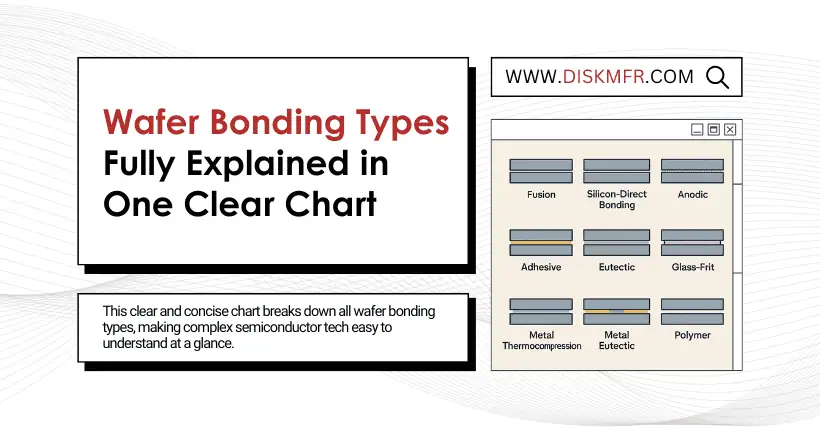
As shown in the image, let’s explain the terms one by one. Permanent bonding is intended to form an irreversible mechanical bond, commonly used in 3D integration, MEMS, TSV, and other device packaging.

01
Temporary Bonding/Debonding
The purpose is to provide temporary support during device processing and be removable later, often used in ultra-thin wafer processing.
Temporary adhesive or carrier wafers are used to bond the thin wafer, and later debonding is achieved through thermal, laser, or chemical methods.
02
Permanent Bonding: Divided into two categories based on the presence of an intermediate layer:
I. Direct Bonding Without Intermediate Layer
- Fusion Bonding / Direct or Molecular Bonding
Principle: Surfaces are bonded through van der Waals forces by ensuring flatness and hydrophilic treatment, followed by annealing to strengthen the bond.
Features: No intermediate material, high bonding strength.
Applications: SOI wafer fabrication, MEMS, Si-Si or SiO₂-SiO₂ bonding. - Cu-Cu / Oxide Hybrid Bonding (Hybrid Bonding)
Principle: Copper atoms bond directly, with dielectric layers (e.g., SiO₂) assisting alignment.
Features: Suitable for high-density 3D packaging, mixed-signal ICs.
Applications: Advanced packaging like TSV, HBM, logic-memory integration using Hybrid Bonding. - Anodic Bonding
Principle: Under high temperature (~300°C) and high electric field, electrostatic attraction and ion migration occur between glass and silicon.
Features: Strong bond, suitable for glass-Si.
Applications: MEMS devices, pressure sensor packaging.
II. Indirect Bonding With Intermediate Layer
(1) Insulating Intermediate Layer
a. Glass Frit Bonding
Principle: Uses low-melting glass paste that flows and bonds under heat.
Applications: Display panels, MEMS.
b. Adhesive Bonding
Principle: Uses organic adhesives like epoxy resin, BCB to bond.
Features: Low requirement on surface flatness, low-temperature process.
Applications: Wafer-level packaging, temporary bonding.
c. Eutectic Bonding
Principle: Uses low melting point of eutectic metal pairs (e.g., Au-Sn) to form a bond.
Applications: MEMS packaging, optoelectronic devices.
(2) Metal Intermediate Layer
a. Reflow Soldering
Principle: Solder like Sn is reflowed under heat to bond with the pads.
Applications: Wafer-level packaging (WLP), micro-bump bonding.
b. Thermocompression Bonding
Principle: High temperature and pressure are used to bond metal layers (e.g., Cu).
Features: Used in high-density packaging, common in TCB process.
Applications: HBM stacking, CoWoS, FO-WLP.

Disclaimer:
- This channel does not make any representations or warranties regarding the availability, accuracy, timeliness, effectiveness, or completeness of any information posted. It hereby disclaims any liability or consequences arising from the use of the information.
- This channel is non-commercial and non-profit. The re-posted content does not signify endorsement of its views or responsibility for its authenticity. It does not intend to constitute any other guidance. This channel is not liable for any inaccuracies or errors in the re-posted or published information, directly or indirectly.
- Some data, materials, text, images, etc., used in this channel are sourced from the internet, and all reposts are duly credited to their sources. If you discover any work that infringes on your intellectual property rights or personal legal interests, please contact us, and we will promptly modify or remove it.


