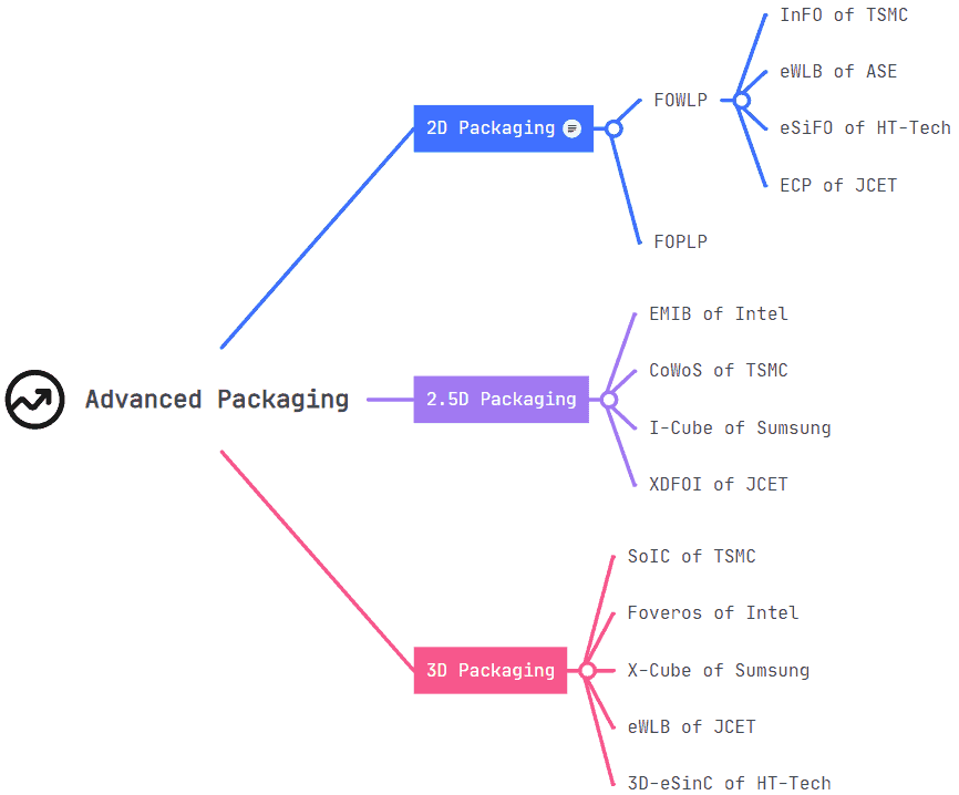
Electronic integration technology is classified into three levels: on-chip integration, in-package integration, and PCB board-level integration. SoC, SiP, and PCB are representative technologies (also called SoP or SoB).
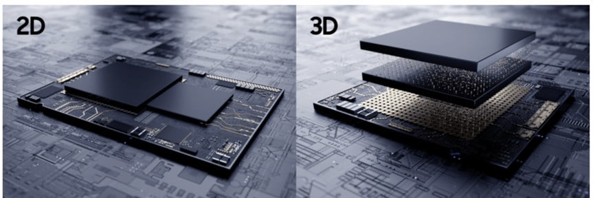
The integration on the chip is primarily 2D, with the transistor tiling integrated into the wafer plane. Similarly, PCB integration is 2D, with electronic components mounted flat on the PCB surface, so both are 2D integration. The situation is much more complicated when it comes to in-package integration.
Two critical criteria for the classification of electronic integration technologies are 1. Physical structure; 2. Electrical connection (electrical interconnection).
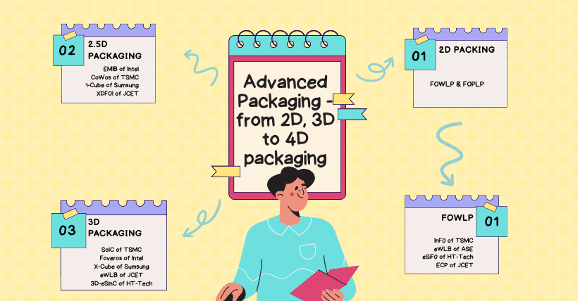
At the moment, advanced packaging can be classified into three types: 2D packaging, 2.5D packaging, and 3D packaging.
💡2D Packaging
An integrated approach in which all chips and passive components are mounted horizontally on the surface of the substrate is referred to as 2D packaging. FOWLP, FOPLP, and other technologies are included in the 2D package.
- Physical Structure: All chips and passive devices are physically installed on the substrate plane. The XY plane is in direct contact with chips and passive devices. Substrate wiring and holes are located below the XY plane.
- Electrical Connection: All electrical connections must pass through the substrate (except for very few bonding points directly connected by bonding wire)
➡️InFO of TSMC
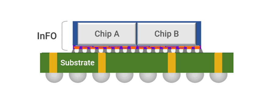
Taiwan Semiconductor Manufacturing created InFO technology in 2017. InFO technology is similar to Fan-out technology used in most packaging plants and can be thought of as the integration of the multi-chip Fan-out process. The main distinction is that the silicon interposer has been removed, and some RDL layers have been used for concatenation (the A10 processor in the 2016 iPhone7, Taiwan Semiconductor 16nm FinFET process, and InFO technology).
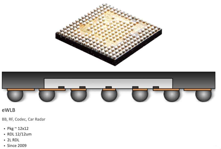
➡️eWLB of ASE
Similar to TSMC InFO, both are Fan-out technologies
In addition, there is a 2D+ integration
2D+ integration refers to the traditional stackable integration of chips connected by bonding lines. Some people may ask, chip stacking is not 3D, why should it be defined as 2D+ integration?
Mainly based on the following two reasons:
- 3D integration now primarily refers to integration via 3D TSV. To avoid misunderstanding, we refer to this traditional chip stacking as 2D+ integration.
- Although the physical structure is 3D, the electrical interconnection must pass through the substrate, which means that the bonding wire must first be bonded to the substrate before the electrical interconnection can take place. This is equivalent to 2D integration. The improvement over 2D integration is stacking in structure, which can save packaging space, so it is called 2D+ integration.
- Physical structure: All chips and passive devices are above the XY plane, some chips do not directly contact the substrate, and the wiring and holes on the substrate are below the XY plane.
- Electrical Connection: All electrical connections must pass through the substrate (except for very few bonding points directly connected by bonding wire)
💡2.5D Packaging
2.5D packaging typically refers to both 2D and partial 3D properties, with representative technologies including Intel EMIB, Taiwan Semiconductor Manufacturing Co., LTD CoWoS, and Samsung I-Cube.
- Physical structure: All chips and passive devices are above the XY plane, and at least some chips and passive devices are installed on the intermediate layer (Interposer). Above the XY plane is the intermediate layer wiring and through holes, and below the XY plane is the substrate wiring and through holes.
- Electrical connection: The Interposer provides the electrical connection of chips located on the intermediary layer.
The Interposer of the intermediary layer is the key to 2.5D integration. In general, there are several scenarios: 1) whether the intermediary layer uses a silicon adapter board, 2) whether the intermediary layer uses TSV, and 3) whether the intermediary layer uses other types of material adapter board; in the case of the silicon adapter, the hole through the intermediate layer is referred to as TSV, and in the case of the glass adapter, it is referred to as TGV.
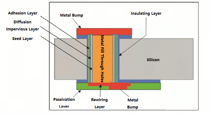
TSV: Through Silicon Via
- Defined as an electrical interconnection structure that links two sides of a silicon wafer and is insulated from the silicon substrate and other through-holes.
- The method of use is: silicon connector and direct use of TSV
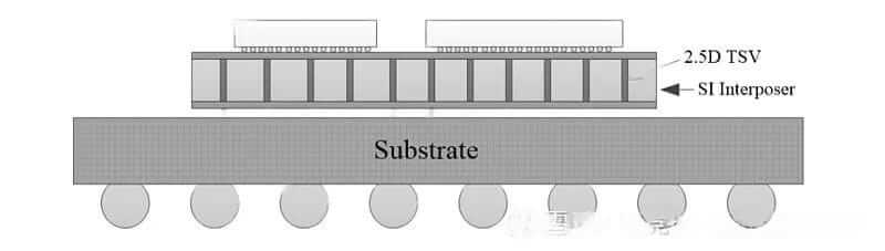
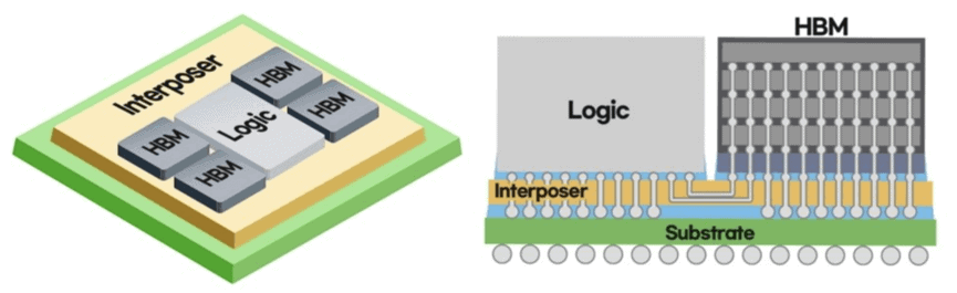
The most common 2.5D integration technology is TSV integration in the silicon intermediate layer. Chips are typically connected to the intermediate layer via MicroBump; the silicon substrate serves as the intermediate layer and is connected to the substrate via Bump; the silicon substrate’s surface is wired via RDL; and TSV serves as the electrical connection channel between the upper and lower surfaces of the silicon substrate. This 2.5D integration is appropriate for large-scale chips with a high pin density. FlipChip chips are typically mounted on silicon substrates.
2.5D integration diagram with TSV:
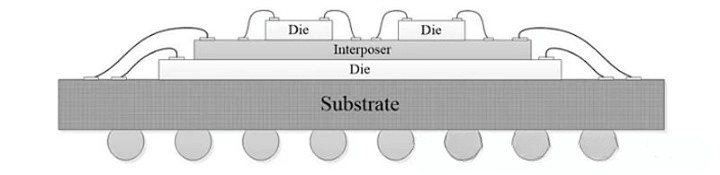
The TSV-free 2.5D integrated structure of the silicon intermediate layer is generally shown as follows. A large bare Chip is directly installed on the substrate, and the connection between the chip and the substrate can be made by Bond Wire or Flip Chip. Multiple smaller bare chips can be installed on top of the large chip due to its large area. But small chips cannot be connected directly to the substrate, so you need to insert an Interposer layer, above which you install multiple bare chips. The intermediary layer has RDL wiring that leads the chip’s signal to the edge of the intermediary layer and then to the substrate via a Bond Wire. This type of intermediary layer usually does not require a TSV, only electrical interconnection via wiring on the upper surface of the Interposer, which is connected by Bond Wire and packaged substrate.
2.5D integration diagram without TSV:
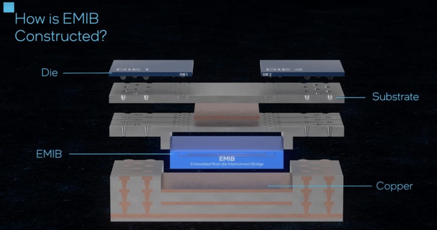
➡️EMIB of Intel
The concept is similar to that of a 2.5D package, but it differs in that there is no TSV. As a result, EMIB technology has the benefits of standard package yield, no additional process, and simple design.
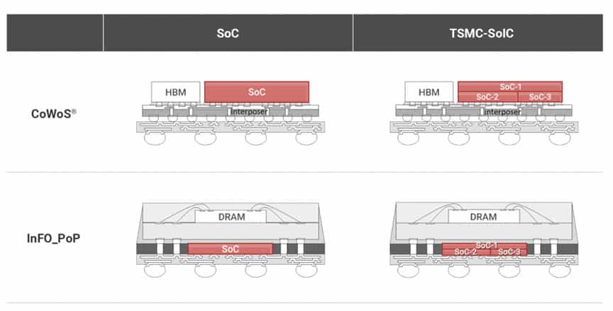
➡️CoWoS of TSMC
CoWoS technology from TSMC is also a 2.5D packaging technology. There are three kinds of intermediate layers: CoWoS S uses Si substrate as the intermediate layer, CoWoS R uses RDL as the intermediate layer, and CoWoS L uses Chiplet and RDL as the intermediate layer.
The TSMC InFO (2D) and CoWoS (2.5D) differ in that CoWoS is aimed at the high-end market and has a greater number of wires and a larger package size. InFO for the cost-effective market, the package size is small, as is the number of connections.
The first-generation CoWoS is primarily employed in large FPGAs. CoWoS-1’s middle layer chip area is approximately 800 mm2, which is very close to the mask limit. Through mask splicing, the second-generation CoWoS significantly expands the size of the intermediate layer. TSMC initially met the 1200mm2 requirement but has since increased the intermediate layer size to 1700mm2. CoWoS-XL2 is the name given to these large packages.
TSMC recently announced that the number of transistors in the fifth generation of CoWoS-S will be increased by 20 times, as will the area of the intermediate layer. In addition, the fifth generation package technology will include eight 128GB HBM2e RAM modules and two large SoC cores.
➡️XDFOI of JCET
It performs better, is more reliable, and is less expensive than 2.5D TSV packaging technology. The system can implement a multi-layer wiring layer with a line distance or online width of up to 2um. Additionally, the package size is enormous and the extremely tiny pitch convex block interconnection technique is used. This allows for the integration of numerous chips, high bandwidth memory, and passive devices.
➡️I-Cube of Samsung
The I, X, R, and H-Cube advanced packages from Samsung are just a few examples. The I-Cube from Samsung also comes in 2.5D.
💡3D Packaging
The fundamental distinction between 3D and 2.5D packaging is that while 3D packaging directly drills and wires on the chip, electrically linking the top and lower chips, 2.5D packaging wires and drills on the Interposer. The term “3D integration” currently largely refers to integration performed exclusively with 3D TSV.
The primary distinction between 3D integration and 2.5D integration is that while 3D integration involves directly drilling (TSV) and wiring (RDL) on the chip, electrically linking the top and lower chips, 2.5D integration involves drilling and wiring on the intermediate layer interposer.
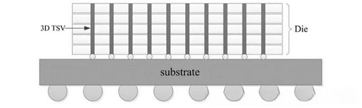
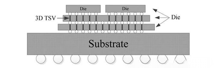
- Physical structure: All chips and passive devices are located above the XY plane. The chips are stacked on top of each other. Above the XY plane, there are TSVS that go through the chip, and below the XY plane, there are wiring and holes for the substrate.
- Electrical connection: Direct electrical connection of the chip through TSV and RDL
In like-chip stacks, where numerous identical chips are stacked vertically next to one another and connected by TSVS that pass through the stack of chips, as seen below, 3D integration is most frequently employed. Memory integration frequently employs similar chip integration techniques, including DRAM stack, FLASH stack, and others.
3D integration diagram of similar chips:
Two different types of chips are typically stacked vertically during the 3D integration of several chips, electrically coupled by TSV, and connected to the lower substrate. On occasion, RDL is etched onto the chip’s surface to connect the top and lower TSVS.
➡️SoIC of TSMC
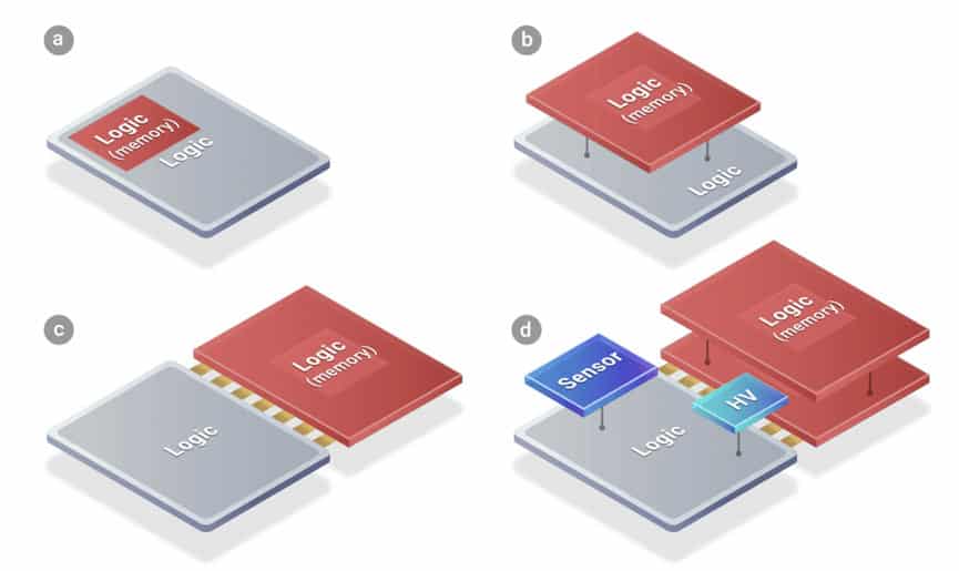
Wafer-on-wafer bonding is a component of 3D packaging, which includes TSMC’s SoIC technology. SoIC is a technology that unites adjacent chips with various features in a bulge-free bonding structure using TSV technology. The bonding material, which is claimed to be valued at up to a billion dollars in secret material, is the key and the portion that is the most enigmatic.
Advanced WLSI can be built using SoIC technology, which combines homogeneous and heterogeneous tiny chips into a single Soc-like chip with a lower size and thinner profile (aka CoWoS and InFO). The newly integrated chip has the necessary heterogeneous integration capabilities built into it, but it appears externally to be a general-purpose SoC processor.
➡️Foveros of Intel
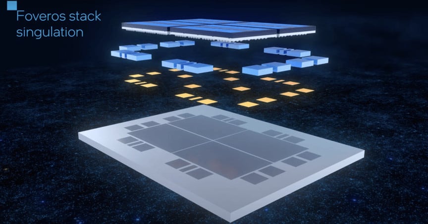
A bottom chip that serves as an active intermediary layer is positioned on the packaging base at the bottom of the 3D Foveros structure. The upper layer of chips and modules may communicate with the rest of the system thanks to a number of TSV 3D silicon holes in the intermediate layer that link the solder bumps up and down.
➡️X-Cube 3D of Samsung
Samsung’s X-Cube test chips, which use their own 7nm EUV process, have been able to stack SRAM layers on top of logic layers and interface with one another through TSV.
➡️eWLB of JCET
With the help of JCET’s EWLB-based intermediate layer, high-density interconnection is possible in a well-developed low-loss package structure, resulting in more effective heat dissipation and quicker processing. Through novel face-to-face bonding, which avoids the requirement for more expensive TSV interconnects while enabling high-bandwidth 3D integration, 3D eWLB interconnects (including silicon segmentation) are realized.
➡️3D-eSinC of HT-Tech
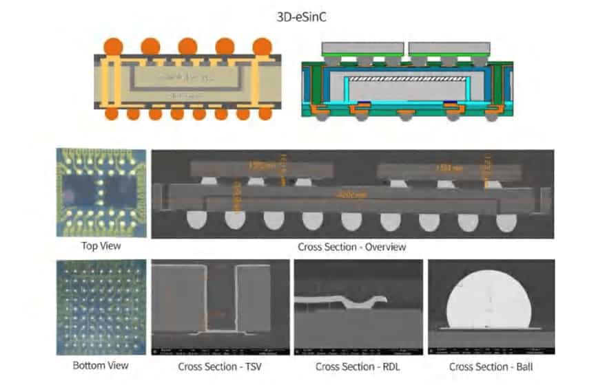
HT-Tech claims that it would introduce cutting-edge packaging innovations such as 2.5D Interpose FCBGA, FOFCBGA, and 3D FOSiP, as well as 3D Memory packaging technology based on the TCB process, in 2022. Research and development of the 12-inch wafer level packaging of car gauge level, the vehicle Lidar technology and goods, and the RF packaging technology of double side molding.
💡4D Integration
- Physical structure: Multiple base plates are installed in a non-parallel manner, each base plate is installed with components, and the installation modes of components are diversified.
- Electrical connection: The substrate is connected by a flexible circuit or welding, and the chip on the substrate is connected by various electrical connections.
4D integration diagram based on rigid and flexible substrate:
The notion of 4D integration encompasses 2D, 2D+, 2.5D, and 3D integration modes since it focuses on the orientation and connections of numerous substrates.