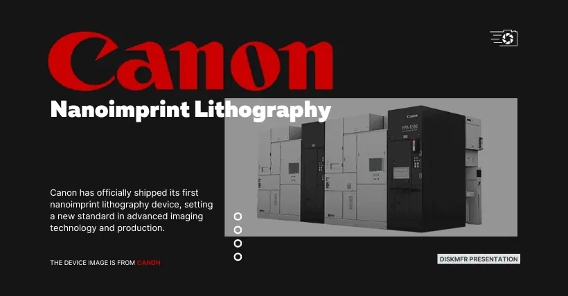
On September 26, 2024, Canon announced the shipment of its advanced nanoimprint lithography (NIL) system, FPA-1200NZ2C, to the Texas Instruments Electronics Research Institute (TIE) based in Texas, USA.
Canon officially launched the world’s first NIL system, FPA-1200NZ2C, on October 13, 2023, becoming the first company to commercialize semiconductor manufacturing systems using NIL technology, which forms circuit patterns differently than traditional projection exposure methods.
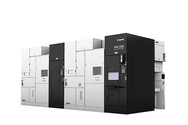
Traditional lithography equipment transfers circuit patterns by projecting them onto photoresist-coated wafers, while the new product achieves this by stamping a mask with the circuit pattern onto the photoresist. This method faithfully reproduces fine circuit patterns on the wafer without using optical components. The new system reduces power consumption and costs, achieving a minimum linewidth of 14nm, comparable to the 5nm node.
Currently, the advanced semiconductor manufacturing equipment market for 5nm processes is dominated by ASML’s EUV lithography machines, priced around $150 million each. For even more advanced 2nm and below processes, ASML has introduced the more expensive High-NA EUV lithography machines, costing up to €350 million, raising the costs required for cutting-edge processes.
In contrast, Canon’s NIL technology allows chip manufacturers to produce logic semiconductors at the minimum 5nm process node without relying on EUV lithography machines. Canon’s semiconductor equipment business director, Kazunari Iwamoto, noted that with improved photomasks, NIL could even produce chips at the 2nm advanced process. Canon’s nanoimprint technology may help close the gap with ASML.
Importantly, Canon’s nanoimprint equipment and manufacturing costs are significantly lower than those of ASML’s EUV lithography machines. Iwamoto mentioned that the costs for customers vary, but estimates suggest the cost for one imprinting process can be halved compared to traditional exposure equipment. Additionally, due to the smaller scale of nanoimprint equipment, it can be more easily adopted for R&D purposes. It is reported that adopting nanoimprint technology could reduce overall equipment investment to 40% of EUV lithography production line equipment costs.
Although Canon has not disclosed the pricing for its nanoimprint equipment, CEO Fujio Mitarai previously stated that the price would be “one digit lower” than ASML’s EUV lithography machines, meaning only 10% higher.
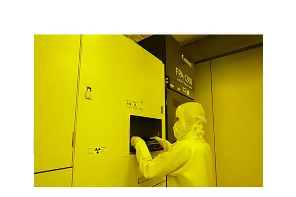
According to Canon’s latest official press release, the first FPA-1200NZ2C will be used at TIE for advanced semiconductor research and prototype production.
TIE is a semiconductor alliance established in 2021, supported by the University of Texas at Austin. It comprises state and local governments, semiconductor companies, national research institutions, and other entities. TIE provides open access to semiconductor R&D programs and prototype design facilities to address issues related to advanced semiconductor technologies, including advanced packaging technologies.
However, it’s important to note that NIL represents a completely different path from lithography technology, making it incompatible with existing DUV or EUV-based production lines. This means that large chip manufacturers cannot directly use NIL technology on their current lines, requiring the establishment of entirely new production lines, which may hinder the promotion of NIL technology. Consequently, the initial customers for Canon’s NIL equipment are primarily research institutions and academic entities.
Moreover, compared to logic semiconductors with dozens of layers of different circuit structures, memory chips, which feature multiple layers of repetitive circuits, are more suitable for manufacturing using NIL technology. This explains the interest from memory chip manufacturers like SK Hynix, Kioxia, and Micron in NIL equipment.
Canon stated that it will continue to advance research and development in semiconductor manufacturing using nanoimprint lithography systems, contributing to the evolution of semiconductor manufacturing technology.

Disclaimer:
- This channel does not make any representations or warranties regarding the availability, accuracy, timeliness, effectiveness, or completeness of any information posted. It hereby disclaims any liability or consequences arising from the use of the information.
- This channel is non-commercial and non-profit. The re-posted content does not signify endorsement of its views or responsibility for its authenticity. It does not intend to constitute any other guidance. This channel is not liable for any inaccuracies or errors in the re-posted or published information, directly or indirectly.
- Some data, materials, text, images, etc., used in this channel are sourced from the internet, and all reposts are duly credited to their sources. If you discover any work that infringes on your intellectual property rights or personal legal interests, please contact us, and we will promptly modify or remove it.


