
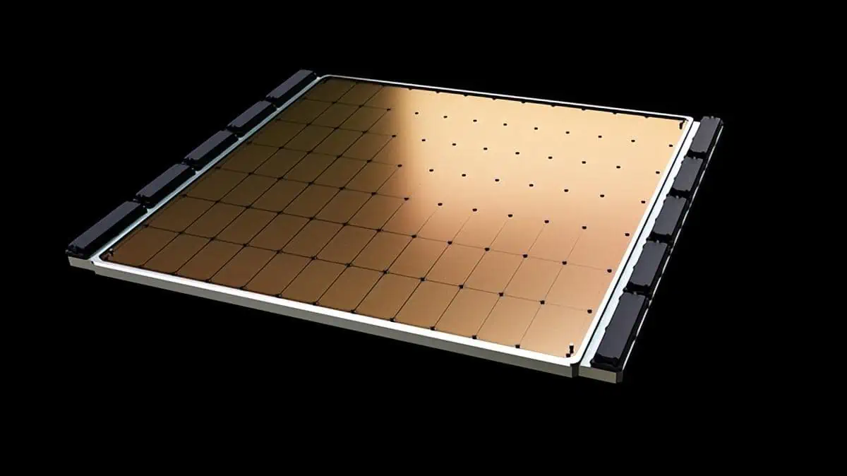
The Institute of Computing Technology of the Chinese Academy of Sciences has already produced a large-scale chip with as many as 256 cores, with the future goal of achieving up to 1600 cores. To accomplish this, the entire wafer will be utilized, known as the ‘wafer-level chip.’
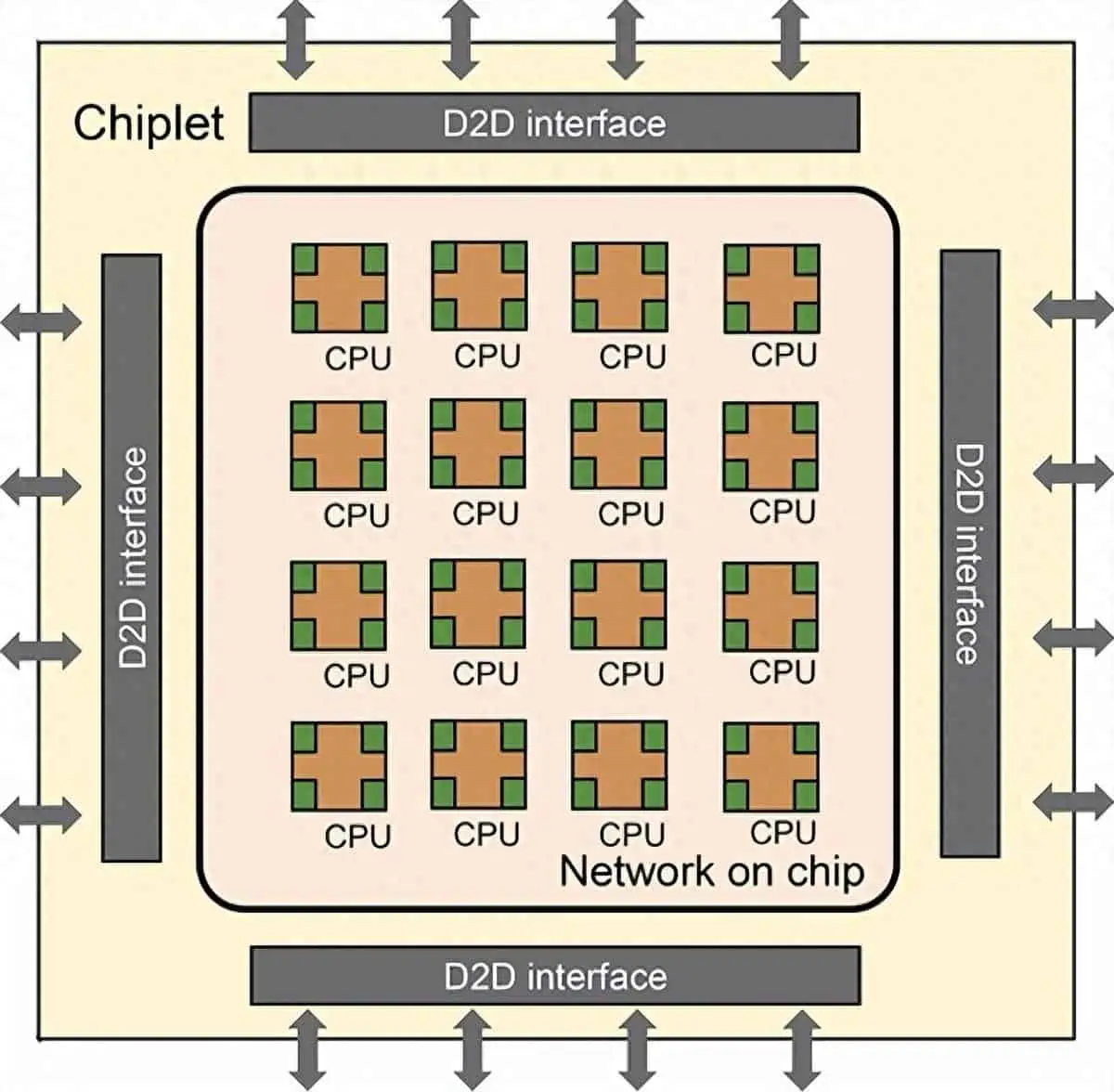
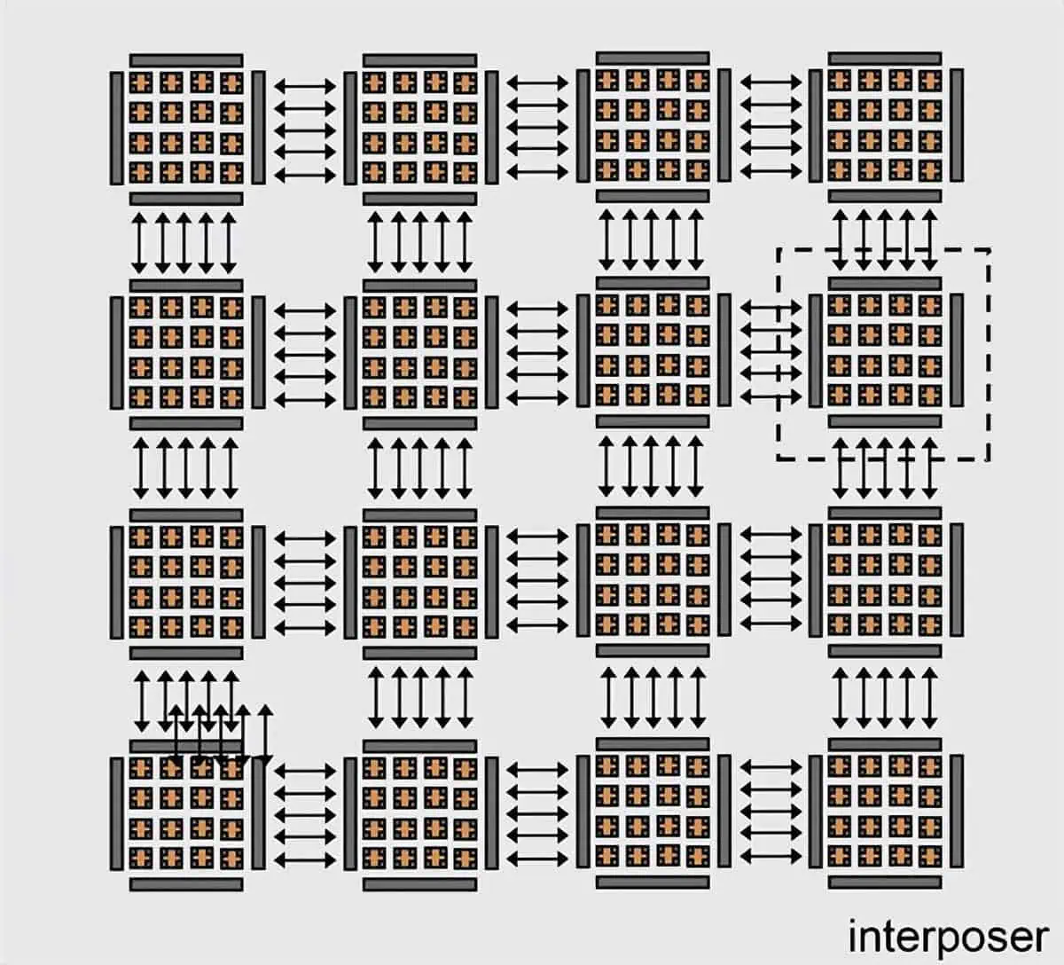
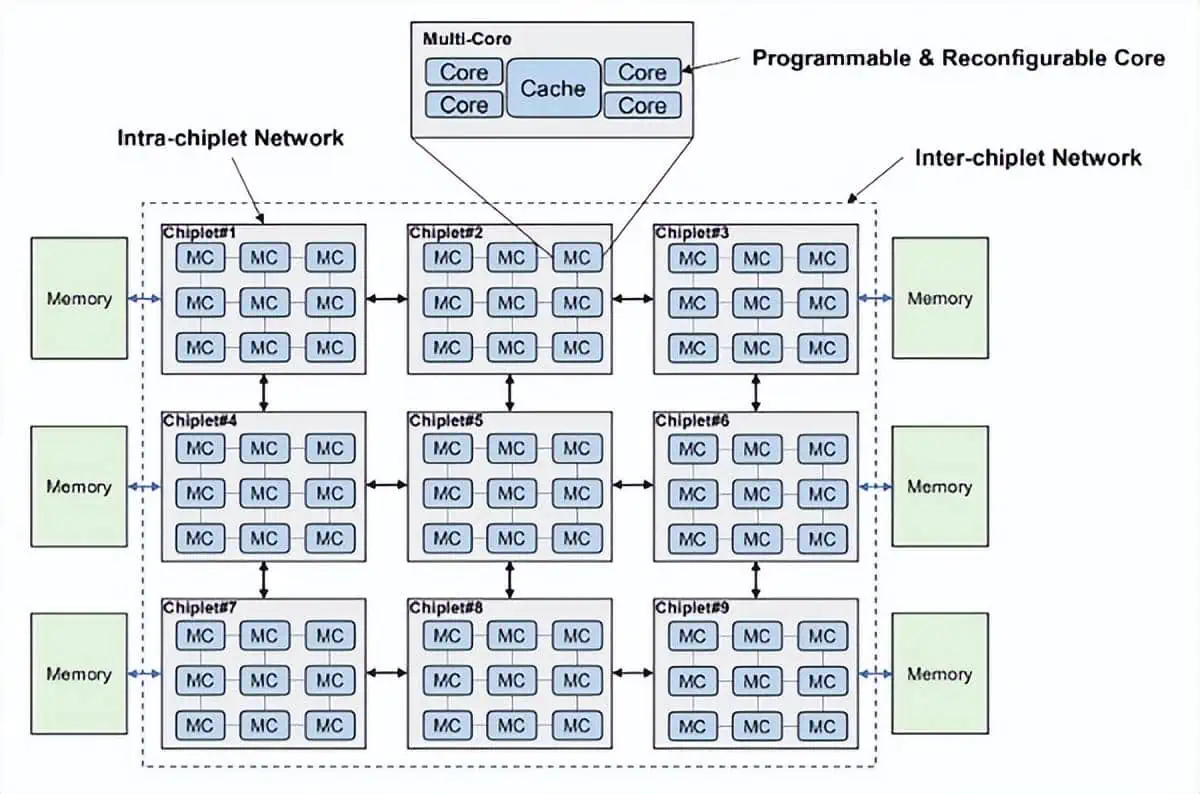
This chip is named ‘Zhejiang‘ and adopts the popular chiplet layout in recent years, divided into 16 chipsets, with 16 RISC-V architecture cores within each chiplet, totaling 256 cores, all supporting programmability and reconfigurability.
Different cores are interconnected through Network-on-Chip (NoC) and Symmetric Multiprocessor (SMP) methods, while interconnections between different chipsets are achieved through Die-to-Die (D2D) interfaces and inter-chipset networks, all connected to the memory jointly and employing a 2.5D intermediate layer package.
In the future, this design can be expanded to 100 chipsets, thereby achieving 1600 cores.
Incredible as it may seem, the manufacturing process is still at 22nm, speculated to be from SMIC. However, despite the remarkably low latency and decent overall performance, the power consumption is not high.
It’s just unknown whether 1600 cores can be achieved under the 22nm process, although SMIC already possesses more advanced processes, hence there are no insurmountable obstacles.
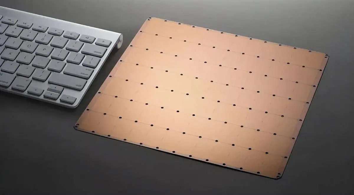
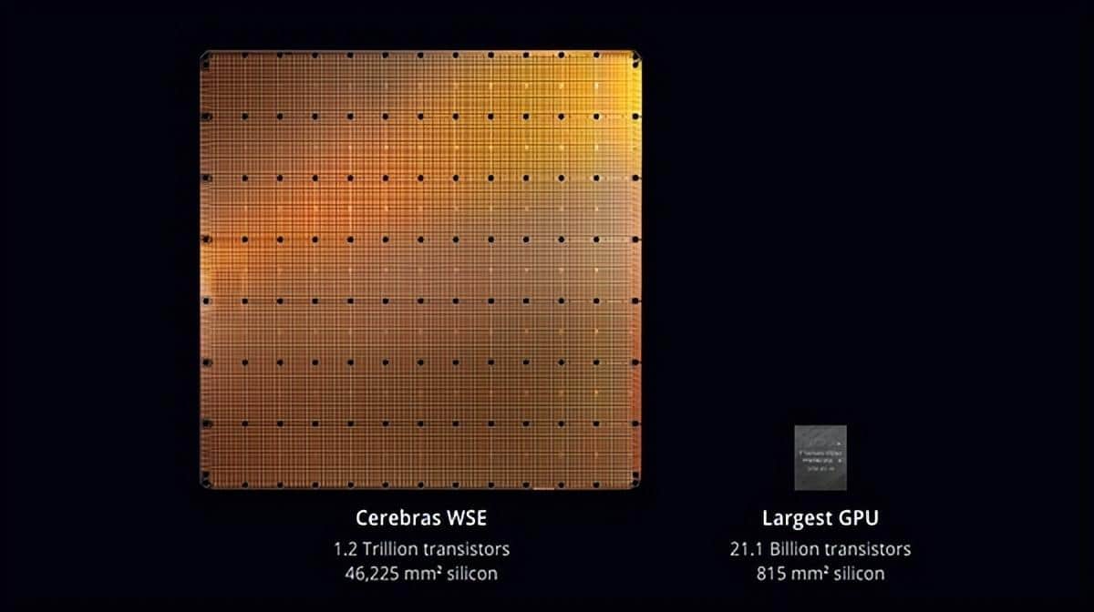
In 2019, semiconductor company Cerebras Systems had already unveiled the world’s largest chip named “WSE” (Wafer Scale Engine), which was as large as a wafer and functioned as an AI processor.
Manufactured using TSMC’s 16nm process, it boasted a surface area of 46225 square millimeters, comprising 1.2 trillion transistors, 400,000 AI cores, 18GB of SRAM cache, 9PB/s of memory bandwidth, and an interconnect bandwidth of 100Pb/s, with power consumption soaring up to 15 kilowatts.
Reportedly, the price tag hovered around several million dollars.

Related:


