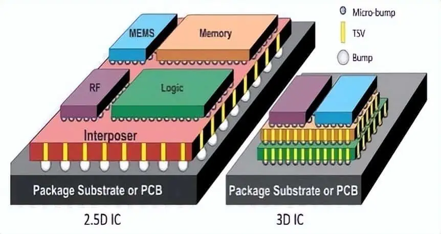
In the process of chip packaging evolving from 2D to 3D, various packaging technologies have emerged. Among them, 2.5D packaging is an advanced heterogeneous chip packaging technology that can achieve a perfect balance between cost, performance, and reliability.
Currently, CoWoS packaging technology has become the preferred choice for many international compute chip manufacturers and is one of the mainstream solutions for high-end performance chip packaging. We believe that the demand growth for NVIDIA’s compute chips has significantly boosted the demand for CoWoS packaging, which is expected to further drive the accelerated development of advanced packaging.
CoWoS technology is a mainstream solution for high-end performance packaging.
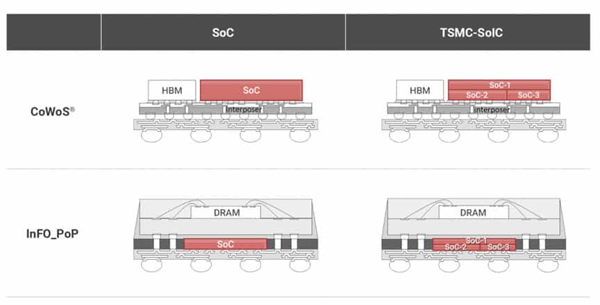
Major global manufacturers are registering independent trademarks for advanced packaging technologies. In recent years, amid the rapid development of advanced packaging, companies developing related technologies have independently named and registered trademarks for their technologies, such as TSMC’s InFO and CoWoS, ASE’s FoCoS, Amkor’s SLIM and SWIFT, Samsung’s I-Cube and H-Cube, and Intel’s Foveros and EMIB. TSMC’s CoWoS technology is one of the mainstream solutions for high-end performance packaging.
We believe that as 2.5D and 3D packaging solutions become increasingly complex, the packaging portfolios of major participants in advanced packaging are also expanding. According to Yole’s “High-End Performance Packaging 2022,” high-end performance packaging platforms include ultra-high-density fan-out packaging (UHD FO), embedded silicon bridge (Embedded Si Bridge), silicon interposer, 3D stack memory, and 3D SoC technology. Embedded silicon bridges have two solutions: LSI (TSMC) and EMIB (Intel). Silicon interposer technologies include TSMC’s CoWoS, Samsung’s X-Cube, and Intel’s Foveros. The combination of EMIB and Foveros has produced CoEMIB technology, mainly used in Intel’s Ponte Vecchio platform. Three-dimensional stack memory is divided into three categories: HBM, 3DS, and 3D NAND stack.

The main advantages of CoWoS are saving space, enhancing interconnectivity between chips, and reducing power consumption.
Over the past decade, CoWoS packaging has undergone five generations of development. Currently, products using CoWoS packaging are mainly distributed in the consumer and server fields, including compute accelerator cards launched by NVIDIA and AMD. CoWoS is applied in the manufacturing process required for NVIDIA GPUs, featuring high technical barriers and significant demand.
At the same time, the CoWoS platform provides best-in-class performance and the highest integration density for high-performance computing applications. This wafer-level system integration platform can offer various interposer sizes, HBM cube quantities, and package sizes. It can achieve mid-layers larger than 2x package size (or about 1,700 square millimeters), integrating leading SoC chips with more than four HBM2/HBM2E cubes.
We believe that CoWoS packaging technology features high integration, high performance, chip combination flexibility, and excellent stability and reliability. As technology continues to advance and market demand grows, CoWoS packaging technology is expected to continue to achieve breakthroughs in the future and be applied in multiple fields.
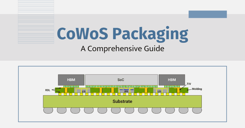
The CoWoS process includes multiple steps. According to Taiwan University, we summarize the CoWoS packaging process into three stages. In the first stage, the die and interposer are connected using micro-bumps (uBump) and underfilled.
In the second stage, the die is connected to the carrier. According to EAB Semiconductor, the package substrate (carrier) is a type of circuit board used to carry the chip, belonging to a technical branch of PCB and is a core semiconductor packaging material. It features high density, high precision, high performance, miniaturization, and thinness, providing support, heat dissipation, and protection for the chip while also offering electrical connection and physical support between the chip and the PCB motherboard. After connecting the die to the carrier, the interposer is thinned using chemical-mechanical polishing (CMP) to remove the recessed parts of the interposer.

In the third stage, the wafer is cut to form chips, which are then connected to the package substrate. Finally, a protective ring and lid are added to the package, and thermal interface materials (TIM) are used to fill the gaps formed when joining with the lid.
CoWoS packaging technology is widely used, currently mainly in high-performance computing, communication networks, image processing, and automotive electronics. In high-performance computing, CoWoS packaging can integrate multiple processor chips, high-speed cache, and memory into the same package, achieving excellent computing performance and data throughput. This feature is critically important in data centers, supercomputers, and artificial intelligence applications. Currently, CoWoS products focus on high-end products with HBM memory modules.
With the rise of the AI wave, the demand for high-performance accelerator cards has significantly increased, and CoWoS mainly targets the high-performance computing (HPC) market, where demand is substantial.
Related:
- TSMC Plans Price Hike for 3nm and CoWoS Technology
- 2025 AI Growth Fuels CoWoS Shortage—Is FOPLP Future?

Disclaimer: This article is created by the original author. The content of the article represents their personal opinions. Our reposting is for sharing and discussion purposes only and does not imply our endorsement or agreement. If you have any objections, please get in touch with us through the provided channels.


