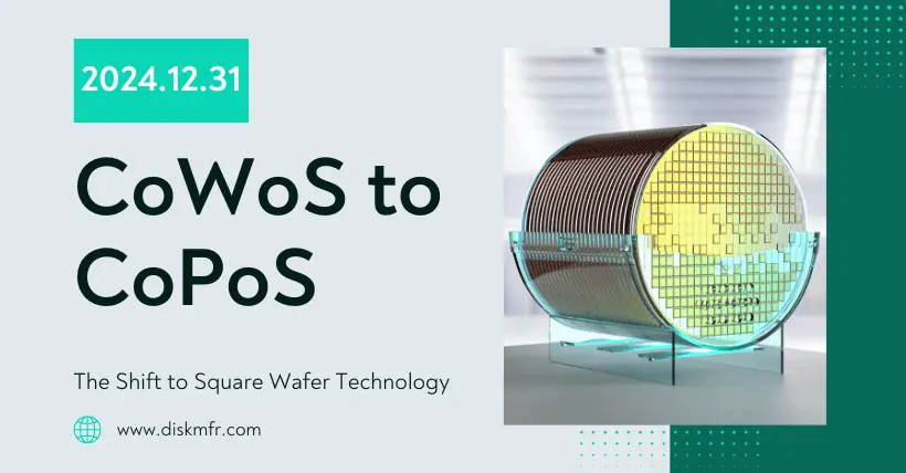
The chip is square, but the wafer is round; what would happen if we replaced the packaging carrier wafer with a square panel?
There was a famous question in the semiconductor section of the Zhihu community: “The chip is square, but why is the wafer round? And why can’t the wafer also be made square?”
Most readers familiar with semiconductor manufacturing should know that this has to do with the Czochralski process for single-crystal silicon wafer production: silicon ingots are cylindrical, and the sliced wafers are therefore round. In fact, the circular shape also has some manufacturing advantages, such as facilitating the uniform application of photoresist and better resistance to edge stress.
For the currently popular fan-out packaging (Fan-out Wafer Level Packaging, FOWLP), once the die (bare chip) on the wafer are prepared, the die are cut and bonded onto another carrier. Usually, the carrier wafer is also round, typically 200mm or 300mm in size, and is sometimes referred to as a “reconstituted wafer” in the industry.
In the advanced FOWLP packaging process, the “wafer level” refers to this round wafer. This part is then used to create the RDL (redistribution layer) as well.
For round wafers with square chips, the biggest drawback is naturally the low area utilization. In the era of rapid development of semiconductor manufacturing and packaging technologies, this might not have been such a significant issue. However, as Moore’s Law stagnates and the cost of advanced manufacturing and packaging processes rises significantly, the area wastage of round wafers has become a more pressing problem.
While it is unlikely that the wafer manufacturing process will change from round to square, why can’t the carrier wafer used in the later stages of packaging be square to improve area utilization and significantly reduce costs? In fact, around the 2010s, PLP (Panel-level Packaging) technology began to gain attention, where the carrier wafer is replaced by a square panel. This way, area utilization could be improved, right?
At last year’s SEMICON China exhibition, we specifically interviewed Manz, a company providing production equipment and solutions for panel-level packaging, about the FOPLP (Fan-out Panel Level Packaging) process. A 12-inch wafer can hold 14 die of 50x54mm size. If a square panel of 510x515mm is used as the carrier, it can hold 4.5 times more die. Moreover, Manz had already begun mass production with even larger panels, including 600x600mm and 700x700mm sizes.
Manz delivered the industry’s largest 700x700mm panel-level packaging production line in 2022.
This year, in addition to FOPLP, Manz has also started discussing CoPoS (Chip-on-Panel-on-Substrate), which replaces the wafer in CoWoS (Chip-on-Wafer-on-Substrate) with a panel. Meanwhile, glass substrate technology has also been brought into focus.
As semiconductor packaging and manufacturing involve upstream and downstream ecosystems and standards, the key to the cost issue lies in whether the end products can be produced at scale. Lin Junsheng, General Manager of Manz Group’s Asia-Pacific region, mentioned at a media conference that PLP panel-level packaging has already achieved mass production in regions like Mainland China, Taiwan, and Southeast Asia. Manz successfully delivered RDL mass production lines in sizes ranging from 300mm to 700mm, and now they are preparing to move into CoPoS, indicating the potential of PLP technology.
Taking this opportunity, this article attempts to discuss the market and future of panel-level packaging technologies.
01
How much opportunity is there in advanced packaging?
Lin Junsheng cited data from Yole Intelligence, which predicts that the advanced packaging market will grow from $37.8 billion in 2023 to $69.5 billion by 2029, with a compound annual growth rate (CAGR) of 11%. In this chart, Yole also clearly defines the scope of “advanced packaging,” which includes flip-chip, fan-out packaging, and the highly discussed 2.5D/3D advanced packaging.
Surprisingly, the 2.5D/3D advanced packaging market reached $10.2 billion last year, and by 2029, it could match the value of flip-chip packaging, with a market CAGR of 15%. Initially, we expected this market to still be in its early stages. This growth is likely due to the current boom in AI, HPC, automotive, and AIPC markets. Particularly, consumer markets like AIPC have begun to widely adopt 2.5D/3D advanced packaging, such as Intel’s Meteor Lake/Lunar Lake and Apple’s M2 Ultra.
The August 2022 issue of Electronic Engineering Times magazine featured an in-depth discussion of advanced packaging technologies. It also mentioned that Apple’s Mx Ultra chip, used in the Mac Studio, employs the InFO-LSI silicon bridge packaging solution, rather than the CoWoS (Chip-on-Wafer-on-Substrate) solution that many had previously speculated.
However, CoWoS has indeed become a key term when discussing advanced packaging in the industry over the past two years—it will also play a critical role in the growth of the 2.5D advanced packaging market value. By the end of 2024, TSMC’s CoWoS monthly production capacity is expected to reach approximately 35,000 wafers, with an annual output of around 300,000–320,000 wafers. It is projected that by 2025, CoWoS monthly capacity will exceed 60,000 wafers. Therefore, from 2022 to 2026, its CAGR is expected to exceed 50%.
As mentioned earlier, from Manz’s perspective, alongside the rapid development of CoWoS, a technology that could partially replace CoWoS is CoPoS (Chip-on-Panel-on-Substrate). By replacing the “W” with “P,” it essentially shifts from wafer to panel, as discussed at the beginning of the article. This not only significantly improves the area utilization of the packaging carrier but also theoretically reduces costs.
This logic is very intuitive and mirrors the relationship between FOWLP (Fan-out Wafer Level Packaging) and FOPLP (Fan-out Panel Level Packaging) that Manz previously discussed. Previously, fan-out packaging wafers could be replaced with panels; now, 2.5D packaging can also replace wafers with panels.
However, we also know that many technologies and even standards related to semiconductor manufacturing and packaging do not undergo changes as easily as simply swapping components. For example, when semiconductor wafers transitioned from 200mm to 300mm, the effort required across the entire industry was enormous; and even with the 450mm wafer, mass production has not yet been realized due to the systemic, ecological, and full industry chain issues involved.
As Lin Junsheng said, in the process of transforming from round to square, “after all, ’round’ has been developed for decades, so changing to ‘square’ is not that easy.” So, can CoWoS to CoPoS really work?
02
What is the current development status of panel-level packaging?
To address this question, it’s essential to first understand the current state of the panel-level packaging market. According to information previously released by Manz, the company has successfully delivered production lines for RDL (redistribution layer) at various sizes, including 300mm, 510mm, 600mm, and 700mm, to several international manufacturers. These lines cover processes such as cleaning, developing, etching, stripping, plating, and automation. What many are more concerned about is which end products are already using chips with panel-level packaging.
A report from TrendForce this year provides an overview of the advanced panel-level packaging market. The chart below shows the direct participants in the panel-level packaging market within the box, while those outside the box are the chip design companies adopting panel-level packaging—i.e., customers of the manufacturers and packagers inside the box.
The bottom layer of the chart indicates that the most widely applied panel-level packaging technology today is for PMIC (Power Management IC), RF ICs, and other chip types, with line widths and pitches typically around 10μm-10μm or 15μm-15μm (chip-first means placing the chip first and then building the RDL layer; chip-last is the opposite). OSAT (Outsourced Semiconductor Assembly and Test) companies, panel manufacturers, and IDMs (Integrated Device Manufacturers) are already widely adopting this technology.
“Traditional packaging methods like wire bonding, QFN, and even flip-chip BGA have shifted towards panel-level packaging. The packaging is smaller, offers better heat dissipation, and has lower costs. Many of our customers are actively adopting this technology for mass production,” said Jian Weiquan, Vice General Manager of Sales for Manz Group in Asia. “With panel sizes as large as 700x700mm, we already have a monthly production capacity of over 10,000 units.”
The middle layer of the chart points to consumer-grade CPUs and GPUs, which are more technically demanding products. Surprisingly, AMD has also shown strong interest in panel-level packaging technology. TrendForce’s market research report from July mentioned that starting from Q2, chip companies, including AMD, have been more actively exploring the use of FOPLP (Fan-out Panel Level Packaging) for consumer-grade chips. At that time, AMD was in discussions with PTI (Powertech Technology) and ASE (Advanced Semiconductor Engineering) about the feasibility of transitioning consumer-grade chips to FOPLP.
Lin Junsheng specifically mentioned that although this market still faces yield challenges, products with line widths and pitches in the range of 5μm to 2μm have already entered “small batch production.”
The top layer of the chart focuses on high-end chips, such as AI GPUs, which are aimed at the HPC (High-Performance Computing) market. These chips tend to have larger chip areas, which makes the shortcomings of wafer-level packaging more evident. In other words, the advantages of panel-level packaging in terms of cost and efficiency are more clearly demonstrated. TrendForce believes that foundries and OSAT companies have already started to explore 2.5D advanced panel-level packaging for this market, “expanding the chip packaging size based on the existing 2.5D model.” However, due to technical challenges, foundries and OSATs “are still evaluating this shift.”
“These chips require even finer line widths and pitches, possibly as small as 2μm-2μm or even 1μm-1μm or below,” Jian Weiquan discussed in an interview. “There are still challenges in achieving panel-level packaging. Whether it’s material selection or equipment, achieving finer line widths and pitches still requires further verification and implementation.” For example, “traditional spin coating cannot be used on large panels, material properties need to be adjusted, and large panels face warping challenges. Exposure precision is affected by depth of focus, and achieving uniform exposure and plating on the entire panel is a problem.”
TrendForce expects that large-scale mass production of FOPLP for consumer-grade chips will begin between the second half of this year and 2026, while AI GPUs will likely not enter large-scale production until 2027-2028. Regarding Manz’s discussion at the media conference about CoPoS (Chip-on-Panel-on-Substrate), which is essentially replacing the “W” (wafer) in CoWoS (Chip-on-Wafer-on-Substrate) with “P” (panel), “this market is just beginning.”
03
Why is CoWoS shifting towards CoPoS?
In other words, Manz regards CoPoS as a new technology that has not fully emerged yet. Before discussing how it may partially replace CoWoS, it’s essential to first understand what CoWoS is. The name “Chip-on-Wafer-on-Substrate” clearly indicates its structure: the die are interconnected via a silicon interposer in the middle layer—this is known as 2.5D packaging. The bottom layer is the substrate.
Manz believes that with the trend toward larger die sizes, such as AI chips potentially reaching 80x84mm, a 12-inch wafer can only accommodate four such die. Furthermore, due to yield issues, the cost per chip would significantly increase. By replacing the “W” with “P” (panel), one can achieve a higher utilization of area and significantly increased capacity.
CoPoS essentially “panelizes” the interposer, creating what’s called Panel RDL (Redistribution Layer) or placing the die on a “panel-level RDL layer.” Even a 510x515mm panel can accommodate several times the number of die that a 300mm wafer can—of course, this doesn’t consider the differences in CoWoS technologies.
From Manz’s description, it seems that CoPoS is likely a solution aimed at partially replacing CoWoS-R (Redistribution Layer Interposer) and CoWoS-L (Local Silicon Interposer). At present, the panels used for packaging large AI chips may still be limited to sizes like 510x515mm, as larger panels present greater challenges in exposure and other processes.
Regarding Silicon Interposers, Manz anticipates that they will transition toward glass interposers. A 2023 article in Electronic Engineering Times mentioned that glass interposers, compared to glass core substrates, represent a more future-oriented technology that requires time to mature.
For traditional BT organic substrates, Manz also believes that glass core substrates are the future. This is likely connected to Intel and Samsung Electronics’ recent announcements about upcoming mass production plans for glass core substrates. Compared to traditional organic substrates, glass core substrates allow for higher interconnection density, more flexible signal routing, fewer RDL layers, higher bandwidth density, and lower power consumption per data transfer. Especially with TGV (Through Glass Via) technology, there is minimal loss, and the material’s properties—such as flatness, CTE (Coefficient of Thermal Expansion), rigidity, moisture absorption, and thermal conductivity—are relatively ideal. It also offers superior mechanical and electrical characteristics, as well as potential for optical transmission applications.
However, the manufacturing of glass core substrates and interposers still presents technical challenges. “The production mode for glass substrates differs from traditional substrates,” explained Dr. Li Yuzheng, Assistant Manager of R&D at Manz Group in Asia. “For example, when using laser processing, the energy cannot be too high, or it will cause cracks. Some cracks are even hard to detect. Therefore, when creating high-density circuits, it is more difficult than with silicon.”
Additionally, the ability to apply the traditional conveyor-based horizontal transfer method used in organic substrates to glass substrates remains uncertain. Mechanical vibrations during transfer could lead to cracks, which would require additional measures. There are also requirements for the circularity and dimensional uniformity of TGV vias.
A well-known large company has also recently showcased glass core substrates based on glass panels in media events. Larger panel sizes enable the production of larger and more glass core substrates, though media were not allowed to take photos, indicating that the technology is still somewhat uncertain in terms of maturity. While Manz did not heavily emphasize glass panels during their media presentation, their press release mentioned “implementing the RDL process on 510mm x 515mm glass substrates for high-bandwidth, high-density D2D (die-to-die) interconnects,” which might be seen as part of the future direction of CoPoS technology.
“Focusing on high-density glass substrates and the co-development of diverse chemicals and process materials, as well as the integration and design of processing equipment, Manz and other equipment manufacturers are deeply invested in glass substrates. This technology is likely close to mass production,” the company notes.
Manz has already developed a TGV via etching system for 510x515mm glass substrates, with product validation expected to be completed with partners by the end of the year. Lin Junsheng mentioned in an interview that although mass production hasn’t been achieved yet, “the industry’s efforts are substantial. Perhaps in 3-4 years, we will see mass production results.”
04
Building an Ecosystem with Partners
Correspondingly, Manz also discussed its actions from the two aforementioned perspectives (including panel-level packaging such as FOPLP/CoPoS and glass substrates). Dr. Li Yuzheng first presented Manz’s overall plan for its clients at the media event, highlighting the company’s expertise in wet processes, including “cleaning, developing, etching, film stripping, electroplating, and automation equipment,” as well as the transmission solutions for processing glass substrates mentioned earlier.
In the complete process, Manz collaborates with its partners—integrating their equipment in processes such as sputtering, coating, and exposure with Manz’s products in key steps to achieve automated integration. “We can provide single-station equipment for clients or integrate front-end and back-end equipment as required, achieving automation connections for automated production.” “We already have a complete Fan-out technology solution for our customers, enabling direct RDL technology mass production.”
Regarding the TGV manufacturing process, Manz has accumulated key processes, including laser modification, TGV chemical etching, surface treatment in the chemical plating process, electroplating, and subsequent RDL processes. This is complemented by the AOI glass inspection and chemical plating Seed Layer deposition with partner equipment to complete the entire process.
Dr. Li Yuzheng specifically introduced Manz’s TGV etching and electroplating equipment. For TGV glass etching, due to the requirements for roundness, uniformity, and via shape, “it is essential to perform inspection after etching.” As a result, Manz currently collaborates with partner equipment for this front-end process. In terms of electroplating, “We have already developed electroplating technology for Fan-out, and subsequently developed double-sided electroplating equipment—currently conducting matching tests with chemical suppliers. We are continuing to make progress in this area with our partners.”
“We are working with equipment and material suppliers throughout the upstream, midstream, and downstream stages to integrate them into a complete supply chain,” said Jian Weiquan. “To achieve process integration and meet customer specifications, we are still in the collaboration and verification phase.”
Combining Manz’s development and product history—starting with PCB and substrate equipment, advancing into display technology development in the new century, accumulating experience with glass materials, and then focusing more resources on packaging technology in the 2010s, with a specific focus on panel-level packaging—Manz officially began developing FOPLP technology in 2012, and by 2016-2017, the technology had yielded results with multiple production lines in mass production.
Given this development history, Manz’s current plans for 2.5D CoPoS packaging and deep involvement in glass core substrates seem entirely reasonable. These two major technical directions also align perfectly with the current trends in AI technology development.
“Very few companies have technical expertise in both substrates and displays,” said Lin Junsheng. “Manz is relatively unique in this regard.” “With the experience accumulated over the past 30 years, we believe we have room to make a significant impact in panel-level technology.” He continued, “Especially with our experience in handling glass, we have an advantage over other equipment manufacturers.” “Combined with our collaboration with other equipment manufacturers and customers, our chances of success are even higher.”

Disclaimer:
- This channel does not make any representations or warranties regarding the availability, accuracy, timeliness, effectiveness, or completeness of any information posted. It hereby disclaims any liability or consequences arising from the use of the information.
- This channel is non-commercial and non-profit. The re-posted content does not signify endorsement of its views or responsibility for its authenticity. It does not intend to constitute any other guidance. This channel is not liable for any inaccuracies or errors in the re-posted or published information, directly or indirectly.
- Some data, materials, text, images, etc., used in this channel are sourced from the internet, and all reposts are duly credited to their sources. If you discover any work that infringes on your intellectual property rights or personal legal interests, please contact us, and we will promptly modify or remove it.


