1. Background of Silicon-Based Photonic Chip Development
Silicon photonic integration technology has become a research hotspot in the past two decades and is internationally recognized as the “microelectronic technology of the 21st century.” With the continuous evolution of optical technology, the functionality of optical systems has become increasingly complex, and their scale has grown. The assembly and calibration difficulties of traditional optical systems based on discrete optical components have become more prominent, highlighting their limitations.
To improve system stability, reduce system size, cost, and power consumption, researchers, inspired by the increasingly mature design approach of integrated circuits, proposed the concept of integrated optical circuits in 1969. Integrated optical circuits involve integrating various optical devices, such as light sources, couplers, modulators, and detectors, onto the same substrate, connected by integrated optical waveguides to form an optical system with more advanced functionality.
Because different materials have different optical properties, researchers have explored various substrate material options to maximize the performance of integrated optical circuits, such as IV-group materials like silicon (Si), silicon dioxide (SiO2), silicon nitride (SiNx), III-V group materials like indium phosphide (InP), indium gallium arsenide phosphide (InGaAsP), aluminum gallium arsenide (AlAsGa), and other novel materials like lithium niobate (LiNbO3) and various polymer materials. Compared to other material systems for photonic integrated chips, silicon-based photonic integrated chips have the following advantages: First, the refractive index contrast between silicon and silicon dioxide is very large, so the optical devices on the SOI platform have strong confinement of the optical field. The size of individual devices and the bending radius of waveguides can be made very small, which is conducive to large-scale integration. Second, silicon is abundant on Earth, and the fabrication process of silicon-based photonic integrated chips is compatible with the complementary metal-oxide semiconductor (CMOS) process used in integrated circuits, offering advantages such as low cost and mass production capabilities. The typical schematic of a silicon-based photonic integrated chip is shown below:
The chip structure is a “silicon-silicon dioxide-silicon” sandwich. The bottom silicon layer, also known as the substrate, supports the entire chip and typically has a thickness of several hundred micrometers. The top silicon layer is used to create optical devices, with a typical thickness of a few hundred nanometers. The buried silicon dioxide layer (Buried oxide, BOX) between them isolates the devices from the substrate to prevent optical field leakage into the substrate, with a thickness typically in the micrometer range.
To protect the top silicon optical devices from oxidation by air, a layer of silicon dioxide cladding is often grown above the top silicon. Through this structure, silicon-based photonic integrated chips can achieve various passive devices such as waveguides, directional couplers (DC), multimode interferometers (MMI), Y-branches, polarization beam splitters/combiners (PBS/PBC), polarization rotators (PR), mode multiplexers, etc. Active devices such as modulators and detectors require additional processes like doping waveguides to form p-n junctions and growing germanium (Ge) materials. In recent years, the technology to grow silicon nitride on the SOI platform has matured, and the integration between SOI and other material platforms is becoming closer.
2. Fabrication of Silicon-Based Photodetectors Based on SOI
For semiconductor silicon-based photodetectors like Ge-on-Si APDs, the design and processes involved must meet process specification requirements. The most commonly used process flow in the specifications is shown below, which simply outlines the main steps in the process design and the distribution of various doped layers.
SOI stands for Silicon on Insulator, a technology that introduces a buried oxide layer (SiO2) between the top silicon layer and the back substrate silicon. The bottom layer is a high-resistance silicon substrate, followed by a high-insulating SiO2 layer. A 220nm single-crystal silicon layer is typically grown next. The top silicon is doped and epitaxially processed. In the process, the single-crystal silicon material can be etched to form various types of waveguides and ridge-type device structures with steps. In standard processes, the etching height is fixed, and only partial etching (70nm, 130nm) or full etching of the 220nm layer is possible. In addition to etching, the 220nm silicon layer can undergo various doping processes at different levels, with standard doping categories such as N++, N+, N, P, P+, P++ etc. Besides forming highly-doped electrode contact layers with fixed doping concentrations, the doping for charge or high-doping expansion areas (N+, N, P, P+) usually has certain range and process limits for dimensions and concentration.
On the 220nm silicon layer, germanium (Ge) materials can also be epitaxially grown. The typical growth thickness for waveguide devices is around 500nm, and for surface incident devices, the growth thickness is generally 720nm. The epitaxial Ge material requires sufficient area and thickness to ensure high-quality Ge. For the epitaxial Ge material, doping is usually limited to electrode contact layer doping, typically N+ and P+ types, to form electrode contact regions. For active devices, vias are formed in the SiO2 insulating layer on the top Si, and metals like W, Al, or Cu are used to fill these vias to form electrodes. The design of the devices requires flexible application of doping and doping characteristics of Si regions, as well as the flexibility of selective epitaxial growth of Ge, to complete the design and fabrication of high-performance silicon-based devices.
The detailed process flow for the Ge-on-Si photodetector design is as shown in the figure, where block region doping is first carried out on the Top Si. The distribution of doped layers in the Si photodetector is shown in Figure 1. Then, Ge is epitaxially grown in the doped Si region, followed by deposition of a layer of SiO2. Part of the SiO2 is etched to form vias for electrode contact layers with the Si, and the first metal filling is carried out, as shown in Figure 2. A second SiO2 deposition and etching to form vias are required, followed by a second metal filling, as shown in Figure 3. Additional processes such as metal contact electrode polishing are performed, completing the Ge-on-Si photodetector fabrication process.
3. Fabrication Process of Silicon-Based Waveguide Structures
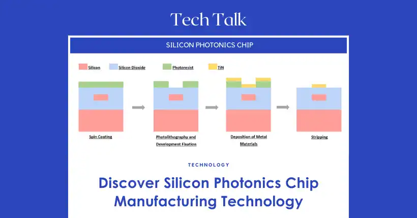
The fabrication process for silicon-based photonic integrated devices is compatible with CMOS processes. The waveguide fabrication process for silicon waveguides is as shown below, which includes: spin coating, photolithography, developing and fixing, etching, resist removal, and cladding deposition.
Before starting the fabrication process, the SOI substrate must first be cleaned to ensure that the silicon wafer surface is free from impurities. After the substrate is dried, the first step is to spin coat the wafer with photoresist. A spin-coater is used to evenly distribute the photoresist on the silicon wafer surface. Then, photolithography is performed to transfer the waveguide pattern to the photoresist. The common methods include electron beam lithography (EBL) and deep ultraviolet (DUV) lithography.
Electron beam lithography uses electron beams to scan the photoresist point by point according to the design layout, which provides high precision but is slow and suitable for small devices with fine structures. In contrast, DUV lithography uses optical masks with waveguide structures to project the optical pattern directly onto the photoresist. This method has lower precision than EBL but is more efficient, lower in cost, and more suitable for commercial large-scale production. After photolithography, the exposed photoresist dissolves in the developer solution, and the silicon layer beneath the dissolved photoresist is exposed.
Using inductively coupled plasma (ICP) etching, the exposed silicon layer can be etched. After etching, the photoresist on the waveguide surface is removed using resist stripping solution, completing the core layer fabrication of the silicon waveguide.
Further, using plasma-enhanced chemical vapor deposition (PECVD), silicon dioxide cladding can be deposited on the chip, completing the fabrication of the silicon-based waveguide. Based on this waveguide structure, titanium nitride (TiN) electrodes can be further grown on the silicon dioxide cladding, completing the fabrication of thermal phase shifters. The detailed process for their fabrication is shown below:
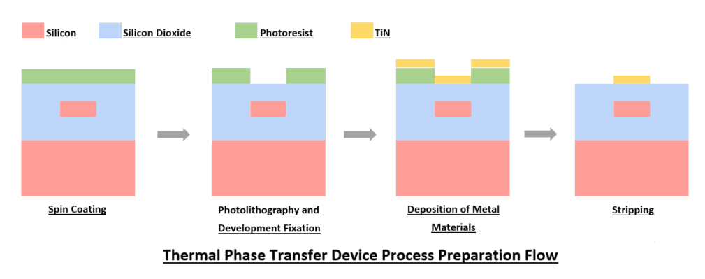
A spin-coater is again used to apply photoresist on the silicon dioxide surface, and photolithography and development are carried out to expose the areas on the silicon dioxide where metal electrodes will be grown. TiN is then deposited using electron beam evaporation or magnetron sputtering. Finally, the chip is immersed in acetone to remove the excess photoresist and metal, completing the growth of the metal electrodes (and thermal phase shifters).
4. Development Status of Silicon-Based Integrated Chips Industry
Silicon-based photonic integrated chips have gained significant attention in the “electronic-optical transmission” data explosion era, making silicon photonics a research focus in both academia and industry. Driven by the microelectronics and optical communications industries, silicon photonic chips have rapidly moved from scientific research to commercialization. In 2007, Luxtera released the world’s first active optical cable (AOC) based on silicon photonic integrated chips, achieving a transmission rate of 40Gb/s and a transmission distance of 300 meters for optical interconnects. In 2014, Acacia released the first silicon photonic coherent transceiver module for metro networks with 100Gb/s. In 2019, Intel released a 400Gb/s silicon photonic transceiver module. In 2020, domestic companies like Alibaba and Hisense also showcased their independently developed 400Gb/s silicon photonic module prototypes. Silicon-based photonic integrated chips play a crucial role in data centers and optical interconnects, effectively addressing massive data exchange challenges.
Currently, the global landscape of companies in the silicon photonics industry is rapidly growing, with an emerging supply chain from R&D, wafer supply, processing, to product release, and the industry is becoming more mature and scalable. Yole predicts that the silicon photonic bare wafer market will surpass $1 billion by 2026, and in addition to the existing optical communications and optical interconnect industries, new sectors like LiDAR, sensing, optical gyroscopes, and quantum computing are also emerging.
References:
(1) Peng Maorong, 2024 Semiconductor Industry Development Issues[C].
(2) Liu Wei, Study of Silicon-Based Reconfigurable Devices and Their Applications in Optical Communications[D].
(3) Zhang Qiongqiong, Research on Photon Communication Technology Based on Single Photon Detection[D].
(4) Zhu Mingyue, Research on High-Speed Fiber Optic Transmission Systems for Metro Data Center Interconnects[D].
(5) Li Yu, Research on Near-Infrared Avalanche Photodetector Chips for Optical Communications[D].
(6) Yuan Weifang, Study on Integrated Micro-Lens Optical Detector Chips for Data Center Applications[D].
(7) Li Yuxuan, Development of Novel Germanium-Silicon Photodetectors[D].
(8) Liu Xiaobin, Development of Novel Germanium-Silicon Avalanche Photodiode Chips[D].
Related:
- AI Pricing Explained: How Token Usage Affects Cost
- Emerging Trends in Silicon Photonics Technology & Progress
- Accelerate AI Innovation with Next-Gen SSD Technology

Disclaimer:
- This channel does not make any representations or warranties regarding the availability, accuracy, timeliness, effectiveness, or completeness of any information posted. It hereby disclaims any liability or consequences arising from the use of the information.
- This channel is non-commercial and non-profit. The re-posted content does not signify endorsement of its views or responsibility for its authenticity. It does not intend to constitute any other guidance. This channel is not liable for any inaccuracies or errors in the re-posted or published information, directly or indirectly.
- Some data, materials, text, images, etc., used in this channel are sourced from the internet, and all reposts are duly credited to their sources. If you discover any work that infringes on your intellectual property rights or personal legal interests, please contact us, and we will promptly modify or remove it.


