The power consumption of EUV lithography machines is a serious issue.
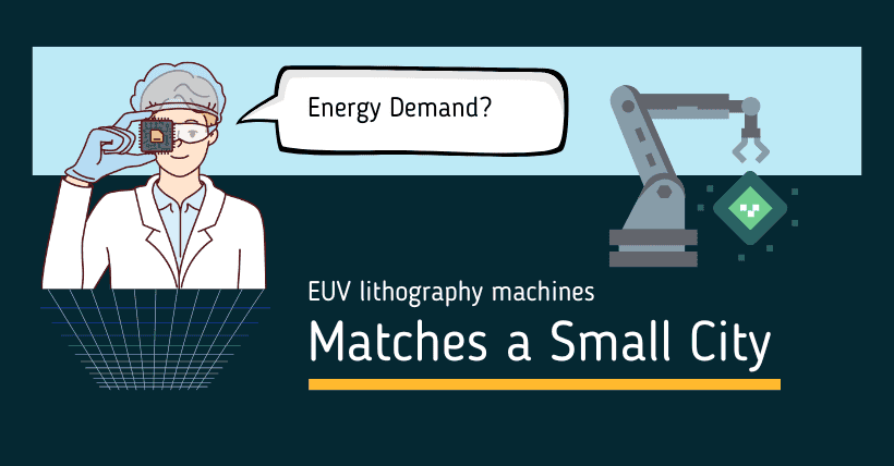
Extreme ultraviolet (EUV) lithography technology is crucial for advanced manufacturing processes and semiconductor production over the next few years. However, each EUV lithography machine consumes 1,400 kilowatts of power (enough to power a small city), making EUV systems major energy consumers with significant environmental impacts. TechInsights estimates that by 2030, the annual electricity consumption of all semiconductor fabs equipped with EUV lithography machines will exceed 54,000 gigawatts (GW)—more than the annual electricity usage of many countries, such as Singapore or Greece.
Current low NA EUV scanners require up to 1,170 kW of power, while the next generation of high NA tools is expected to need up to 1,400 kW per unit (according to TechInsights). The number of these machines installed in fabs operated by Intel, Micron, Samsung, SK Hynix, and, of course, TSMC, is increasing each year.
TechInsights projects that by 2030, the number of fabs equipped with EUV scanners will grow from 31 to 59, approximately doubling the number of operational machines. Consequently, all installed EUV systems will consume 6,100 GW of power annually, which is comparable to Luxembourg’s yearly consumption. Although 6,100 GW is not excessively high, each advanced chip requires over 4,000 manufacturing steps, and fabs house hundreds of different tools. EUV devices account for roughly 11% of a fab’s total power consumption, with the remaining energy used by other tools, HVAC systems, facility systems, and cooling equipment. Therefore, the total power consumption of all fabs equipped with low NA and high NA EUV lithography machines is estimated to rise to 54,000 GW per year.
Specifically, 54,000 gigawatts per year is about five times the electricity consumed by Meta’s data centers in 2023. This amount also exceeds the annual consumption of Singapore, Greece, or Romania and is over 19 times the annual electricity usage of the Las Vegas Strip. Yet, despite its magnitude, it only accounts for 0.21% of the global electricity consumption in 2021 (25,343,000 gigawatts per year), a relatively small share.
If 59 state-of-the-art semiconductor facilities equipped with EUV lithography machines consume 54,000 GW per year, each facility would consume an average of 915 GW per year, comparable to the power usage of advanced data centers.
The number of EUV-equipped fabs is expected to nearly double by 2030, with power consumption more than doubling as well. Power infrastructure will face major challenges, as even today, companies like AWS, Google, Meta, and Microsoft struggle to find locations to build megawatt- and gigawatt-level data centers that the grid can support.
Today, chip manufacturers like Intel prefer to use only sustainable green energy, though their current power consumption remains limited. As AI data centers continue to demand more power, AWS, Microsoft, and Oracle are planning to power their data centers with nuclear power plants. Perhaps in a few years, chip manufacturers may also have to consider nuclear power. However, whether the grid will be able to supply power for AI data centers, advanced fabs, homes, and other industries within just six years remains to be seen.
TechInsights concludes: “To ensure a sustainable future, the industry needs to invest in energy-efficient technologies, explore renewable energy sources, and work with policymakers to address power infrastructure challenges. In doing so, they will be able to expand semiconductor power while minimizing environmental impact.”
Japan Develops New EUV Lithography Technology, Cutting Power Consumption by 90%
Okinawa Institute of Science and Technology in Japan has developed a technology that significantly reduces the power consumption and manufacturing costs of EUV lithography equipment needed to produce cutting-edge semiconductors. This technology reduces the number of mirrors in the EUV path from 10 to 4, dramatically cutting the power requirements of the EUV light source. The university aims to collaborate with companies to realize domestic production of this equipment in Japan.
This new technology was developed by Professor Tsui of Okinawa Institute of Science and Technology. Currently, EUV lithography equipment is exclusively supplied by ASML, the Dutch semiconductor equipment giant. The existing equipment uses a laser to generate EUV, which is then reflected through 10 mirrors to reach the wafer and transfer the circuit pattern—a highly complex process.
EUV energy decays by 40% with each reflection, so ultimately, only about 1% of the energy reaches the wafer. In contrast, the new technology uses only four mirrors, allowing more than 10% of the energy to reach the wafer. With the EUV light source as the focus, overall power consumption can be reduced to about one-tenth of current levels. The simplified equipment structure also significantly reduces the estimated 20 billion yen introduction cost by nearly half.
In the future, Okinawa Institute of Science and Technology will conduct verification tests using a half-size device with LEDs, followed by EUV testing from 2025. Professor Tsui stated, “We hope to work with companies to develop the first device by as early as 2026.”
Related:

Disclaimer:
- This channel does not make any representations or warranties regarding the availability, accuracy, timeliness, effectiveness, or completeness of any information posted. It hereby disclaims any liability or consequences arising from the use of the information.
- This channel is non-commercial and non-profit. The re-posted content does not signify endorsement of its views or responsibility for its authenticity. It does not intend to constitute any other guidance. This channel is not liable for any inaccuracies or errors in the re-posted or published information, directly or indirectly.
- Some data, materials, text, images, etc., used in this channel are sourced from the internet, and all reposts are duly credited to their sources. If you discover any work that infringes on your intellectual property rights or personal legal interests, please contact us, and we will promptly modify or remove it.


