01
Why Slice Semiconductor Wafers?
Wafer slicing is the process of dividing an entire wafer into individual chips. This step is critical not only for chip size precision and edge quality but also directly affects packaging, testing efficiency, and yield rates. With the rapid advancement of semiconductor technology, wafer sizes are increasing, prompting advancements in slicing techniques to meet demands for higher precision and lower damage.
02
Mechanical Semiconductor Wafer Slicing
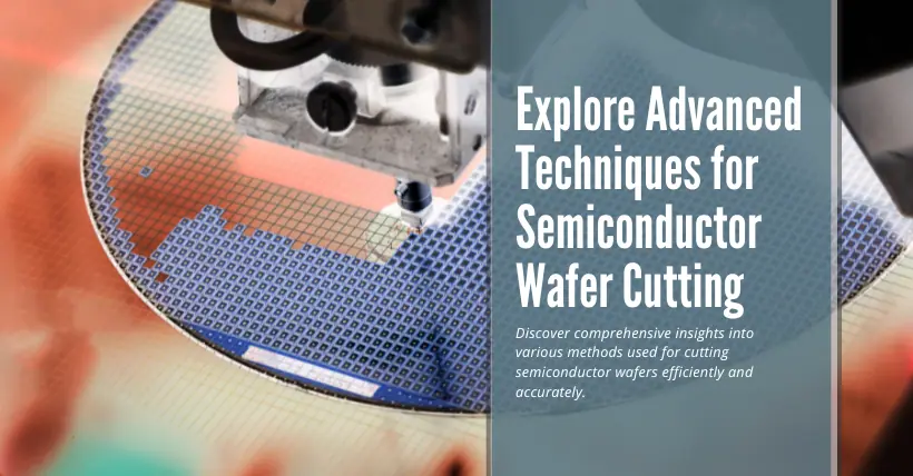
Mechanical wafer slicing is one of the most traditional and commonly used methods, dating back to the early days of the semiconductor industry. This method utilizes high-speed rotating diamond blades to physically separate the wafer into individual chips. The blades spin rapidly over the wafer surface while the wafer is securely held on a precise worktable, achieving separation through relative motion. Blade hardness and sharpness are crucial for ensuring cutting quality. Additionally, to minimize heat and debris effects on the wafer during cutting, water or other cooling media are often used.
Mechanical slicing offers advantages such as low equipment costs and suitability for processing wafers of various materials. However, it has drawbacks including relatively lower slicing precision, slower rates, and susceptibility to edge chipping, especially with thinner wafers. It also requires skilled operators to precisely control cutting force and speed.
03
Laser Wafer Slicing
With the rapid development of laser technology, laser wafer slicing has emerged as a favored method in the wafer slicing domain. Known for its high precision, efficiency, and minimal damage, laser slicing has gained prominence in high-end semiconductor manufacturing. Laser slicing can be categorized into laser stealth dicing and laser full cutting.
① Laser Stealth Dicing
Laser stealth dicing is an innovative wafer slicing technique that involves forming modification layers inside the wafer using laser beams, rather than cutting directly on the surface. This process includes focusing the laser beam inside the wafer to create fine cracks or modification layers. Subsequently, a mechanical process stretches and peels the tape applied to the back of the wafer, naturally separating it along the pre-cut laser path.
The advantages of laser stealth dicing include avoiding stress damage and edge chipping caused by surface cutting, improving chip edge quality and yield. However, it comes with limitations such as high equipment costs and the need for multiple processing steps to completely separate thicker wafers.
② Laser Full Cutting
In contrast to stealth dicing, laser full cutting directly utilizes laser beams on the wafer surface, penetrating its entire thickness to achieve complete chip separation. This technique adjusts laser power, focus, and speed precisely to accommodate different materials and wafer thicknesses.
The benefits of laser full cutting include extremely high cutting speeds, minimal stress damage, and exceptional cutting precision. It eliminates tool wear and mechanical stress issues associated with traditional methods. However, challenges include high costs and difficulties in clearing burnt debris.
04
Latest Advances in Laser Slicing Technology
As laser technology continues to advance, its applications in semiconductor manufacturing expand. Recent developments in ultrafast lasers (such as picosecond and femtosecond lasers) have brought new breakthroughs to laser slicing technology.
① Application of Ultrafast Lasers
Ultrafast lasers, characterized by their extremely short pulse durations (picoseconds to femtoseconds) and high peak powers, concentrate laser energy within very small areas inside the wafer. This capability enables high-precision, low-damage processing in both stealth dicing and full cutting methods. By precisely controlling laser focus depth and energy distribution, ultrafast lasers achieve precise modification layers inside wafers or high-precision surface cutting.
② Exploration of New Laser Cutting Techniques
Beyond ultrafast lasers, researchers are exploring new laser cutting techniques to enhance wafer slicing efficiency and quality. For example, Disco Corporation in Japan has developed the Key Amorphous Black Repetitive Absorption (KABRA) technology, an innovative laser cutting method. This technique focuses laser energy inside silicon carbide materials to induce “amorphous black repetitive absorption,” breaking down silicon carbide into amorphous silicon and amorphous carbon layers, forming a black amorphous layer as a separation point for wafers. This technology improves production efficiency and reduces thermal effects and residual stress during processing.
Related:
- What Is a Seal Ring in Semiconductor Chips Exactly?
- How Wafer Sawing Boosts Chip Yield and Reliability?
- How to Remove Epoxy Resin from Plastic Chip Packages?

Disclaimer:
- This channel does not make any representations or warranties regarding the availability, accuracy, timeliness, effectiveness, or completeness of any information posted. It hereby disclaims any liability or consequences arising from the use of the information.
- This channel is non-commercial and non-profit. The re-posted content does not signify endorsement of its views or responsibility for its authenticity. It does not intend to constitute any other guidance. This channel is not liable for any inaccuracies or errors in the re-posted or published information, directly or indirectly.
- Some data, materials, text, images, etc., used in this channel are sourced from the internet, and all reposts are duly credited to their sources. If you discover any work that infringes on your intellectual property rights or personal legal interests, please contact us, and we will promptly modify or remove it.


