I. Introduction
Charge carriers are a core concept in electricity and electronics. They refer to the microscopic particles that carry charge and participate in current conduction in conductive materials. Their properties and characteristics directly determine the physical properties of materials, such as electrical conductivity, thermal conductivity, and optoelectronic properties.
II. Definition and Nature of Charge Carriers
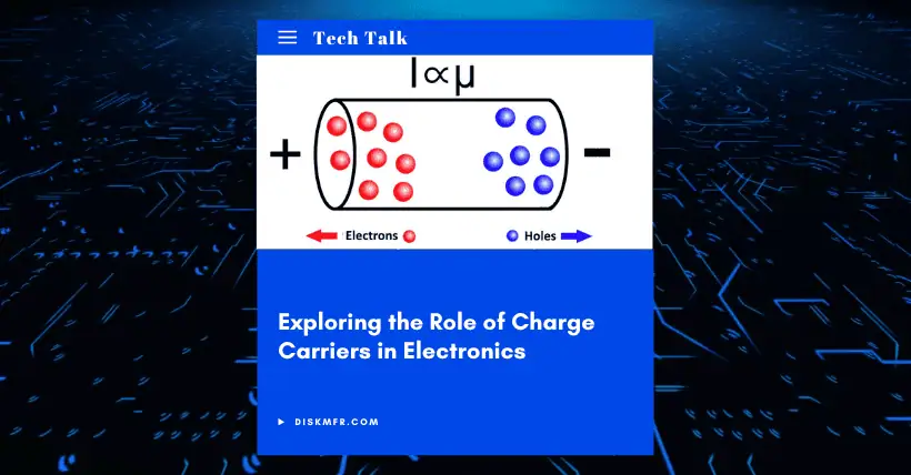
In semiconductor materials, there are two main types of charge carriers: electrons and holes. Both electrons and holes can participate in conduction, and their quantity and motion characteristics determine the electrical properties of the semiconductor.
In pure semiconductors, due to thermal excitation and other reasons, a small number of electrons gain enough energy to break free from covalent bonds and become free electrons. At the same time, a vacancy is left at the position of the original covalent bond, which is called a hole.
Although holes themselves do not carry a negative charge, they can be regarded as positively charged particles because when adjacent atoms’ valence electrons fill the hole, it is equivalent to the hole moving in the opposite direction of the electron.
III. Generation of Charge Carriers
Charge carriers are typically generated through three mechanisms: thermal excitation, optical excitation, and doping.
In semiconductors, introducing impurity atoms (doping) is a common and effective method to control the carrier concentration. Depending on the properties of the impurity atoms, doping can be classified into N-type and P-type doping.
N-type doping generally introduces pentavalent elements (such as phosphorus (P), arsenic (As), etc.) into the semiconductor. These pentavalent elements contribute an extra electron to the semiconductor lattice, which easily becomes a free electron, thus increasing the concentration of electrons in the semiconductor. At this point, electrons become the majority carriers, and holes become minority carriers.
P-type doping involves introducing trivalent elements (such as boron (B), gallium (Ga), etc.). These trivalent elements create a hole in the lattice, increasing the concentration of holes and making holes the majority carriers, with electrons becoming the minority carriers. By precisely controlling the type and concentration of doping, the electrical properties of semiconductors can be finely tuned to meet the needs of different electronic devices.
IV. Recombination of Charge Carriers
The recombination of charge carriers is the opposite process to their generation. When an electron and a hole meet, the electron will fill the hole, causing them to disappear. This process is called recombination, and it releases energy, which can be in the form of photons or heat.
In semiconductor devices, the recombination process significantly affects device performance. For example, in light-emitting diodes (LEDs), by controlling the recombination process of electrons and holes, they can recombine in a radiative manner to release photons, thereby achieving light emission.
V. Drift/Diffusion and Scattering of Charge Carriers
✅ Drift
The drift of charge carriers refers to the process in which free electrons or holes in a semiconductor or conductor accelerate in the direction of the applied electric field. Drift motion is one of the fundamental mechanisms for the formation of current.
Mobility is a physical quantity that describes how easily charge carriers can migrate, reflecting the average drift velocity of carriers under a unit electric field. The mobility of different types of charge carriers in the same material is usually different.
By optimizing material quality, controlling the electric field distribution, and lowering temperature, the drift velocity of charge carriers can be effectively increased, thus enhancing the efficiency of semiconductor devices.
✅ Diffusion
Even in the absence of an electric field, charge carriers will diffuse due to concentration gradients. When the concentration of charge carriers in a certain region of a semiconductor is higher than in other regions, the charge carriers will diffuse from the high-concentration region to the low-concentration region to achieve a uniform concentration distribution.
For example, in a PN junction, due to the difference in carrier concentration between the P region and the N region, electrons and holes will diffuse, forming an internal electric field in the junction. This internal electric field has a decisive effect on the electrical properties of the PN junction, such as its unidirectional conductivity.
✅ Scattering
During their motion, charge carriers will collide with lattice vibrations, impurity atoms, or other charge carriers, resulting in energy loss and a change in motion direction. This scattering effect reduces the mobility of charge carriers, which in turn affects the electrical conductivity of the material.
VI. Applications of Charge Carriers
Semiconductor devices are the core of modern electronic technology, and charge carriers play a crucial role in them. Take transistors, for example. Whether it is the common bipolar junction transistor (BJT) or the field-effect transistor (FET), their operation principles are based on the movement and control of charge carriers.
In a bipolar junction transistor, the base current controls the transport of charge carriers (electrons and holes) between the emitter and the collector, enabling signal amplification and switching functions. In a field-effect transistor, the gate voltage controls the concentration and migration of charge carriers in the channel, thus controlling the current.
Integrated circuits, which integrate large numbers of transistors and other semiconductor devices on a single chip, use precise control and transmission of charge carriers in these devices to achieve complex logic operations, data storage, and processing functions, driving the rapid development of fields like computing and communication.
VII. Conclusion
Charge carriers, as the key determining factor of a material’s electrical properties, play a vital role in the generation, recombination, migration, diffusion, and scattering behaviors, as well as in the applications across various materials and devices. These behaviors form the crucial foundation of modern physics and electronics.
Related:
- eSIM Explained Simply: What It Is and How It Works
- 1g of Silver Nanowire Can Wrap Around Earth 5 Times

Disclaimer:
- This channel does not make any representations or warranties regarding the availability, accuracy, timeliness, effectiveness, or completeness of any information posted. It hereby disclaims any liability or consequences arising from the use of the information.
- This channel is non-commercial and non-profit. The re-posted content does not signify endorsement of its views or responsibility for its authenticity. It does not intend to constitute any other guidance. This channel is not liable for any inaccuracies or errors in the re-posted or published information, directly or indirectly.
- Some data, materials, text, images, etc., used in this channel are sourced from the internet, and all reposts are duly credited to their sources. If you discover any work that infringes on your intellectual property rights or personal legal interests, please contact us, and we will promptly modify or remove it.


