In the field of precision processing in the microscopic world, Focused Ion Beam (FIB) technology is like a magical “nano-sculptor,” opening new paths for material processing, analysis, and imaging through its unique technical means. By delicately manipulating ion beams, this technology enables nanoscale precision operations and demonstrates vast application potential across multiple fields.
01
Core Concept of FIB Technology
FIB technology utilizes a highly focused ion beam as a “precision tool,” where accelerated and precisely controlled ions interact with the surface of a sample to achieve nanoscale material processing goals. In practice, gallium (Ga) ion sources are commonly used in FIB systems due to their excellent focusing performance and suitable mass, meeting the requirements of most application scenarios.
02
Basic Structure of an FIB System
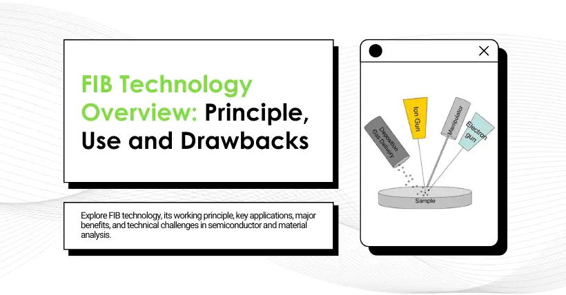
- Ion Source: As the “power source” of the FIB system, the ion source generates ion streams to bombard the sample. The liquid metal ion source, especially liquid gallium, is the most widely used due to its low melting point, low vapor pressure, and excellent chemical resistance. By heating the metal into a liquid and forming a sharp emission tip, single or few ions are extracted precisely under a strong electric field. The ion source, located at the top of the system, is the heart of FIB technology.
- Acceleration and Deflection System: This system acts as the “navigator” of the ion beam, providing ions with the necessary kinetic energy and controlling the direction and shape of the beam via electric or magnetic fields to ensure accurate targeting.
- Sample Chamber: This “dedicated space” holds the sample to be processed. It is usually maintained under high vacuum to preserve beam quality and performance, avoiding external interference with the ion-sample interaction.
- Detection System: Responsible for collecting and analyzing various signals produced during ion-sample interaction, such as secondary ions and secondary electrons. These signals provide abundant information about the sample.
03
Working Principle of FIB Technology
- Ion Generation and Acceleration: The ion source is the key place for ion production. Taking liquid gallium as an example, the metal is heated to a liquid state and forms an ion emission point at the tip. Extracted ions are accelerated through thousands of volts to gain sufficient energy for subsequent interactions with the sample.
- Focusing and Scanning of Ion Beam: The accelerated ion beam is refined through a focusing system composed of electromagnetic lenses, narrowing it to nanoscale precision. The beam diameter can vary from a few to hundreds of nanometers. The deflection system changes the ion beam direction via voltage or current, allowing it to scan the sample surface precisely along a preset path.
- Interaction with Sample:
- Etching Mechanism: When a high-energy ion beam hits the sample, physical sputtering occurs. Incident ions transfer energy to surface atoms, ejecting them and enabling fine cutting, drilling, and sculpting to form complex microstructures.
- Deposition Mechanism: Under certain conditions, FIB can also deposit new materials. Specific gas precursors introduced into the chamber decompose under ion bombardment, forming thin films on the sample surface—used in circuit repair and conductive connection creation.
- Imaging Mechanism: Ion impacts produce signals such as secondary electrons and backscattered ions. These are detected to generate surface morphology images, similar to scanning electron microscopy. Modern dual-beam systems combine SEM functions to enhance image quality.
04
Versatile Functions of FIB Technology
- Etching Function: In microelectronics manufacturing and repair, FIB’s etching capabilities enable precise nanoscale cutting and drilling. It can locate and remove faulty circuit parts in the semiconductor industry, assisting in failure analysis.
- Deposition Function: FIB also adds material. By decomposing and depositing gas precursors, it repairs damaged circuits and creates conductive paths, offering more possibilities in material processing.
- TEM Sample Preparation: FIB can extract ultra-thin slices only tens of nanometers thick from bulk material, ideal for observing internal structures with TEM, especially suitable for hard or brittle materials.
- Imaging Function: FIB observes surface morphology using interaction signals, although its resolution is slightly lower than SEM. Dual-beam systems integrate high-resolution imaging with precise processing.
- Tomography and 3D Reconstruction: Continuous section imaging allows 3D modeling of a sample’s internal structure—useful for studying complex material microstructures such as chip interconnects and cellular relationships in biological tissues.
- Nano-Manipulation and Assembly: In nanotechnology, FIB allows precise manipulation of single nanoparticles or nanowires—moving, welding, or cutting them—to advance nanotech research and development.
- Material Modification: Through local doping or chemical composition adjustment, FIB alters surface properties, optimizing physical characteristics like electrical and optical properties, aiding new material development.
05
Advantages and Limitations of FIB Technology
(1) Significant Advantages
- High Precision: Nanoscale resolution and positioning accuracy make it ideal for micro-nano manufacturing and fine processing.
- Multi-functionality: One device can perform etching, deposition, and imaging, simplifying procedures.
- Rapid Prototyping: No need for traditional masks, speeding up R&D and design validation.
- Localized Processing: Operates on specific areas without affecting surroundings, preserving material integrity.
- Material Modification: Effectively enhances material performance.
- TEM Sample Preparation: Excellent for preparing TEM samples, especially for special materials.
- Efficiency of Dual-Beam Systems: Combines SEM for higher work efficiency and timely result inspection.
(2) Limitations
- High Cost: Equipment purchase, operation, and maintenance costs are high, limiting widespread adoption.
- Slow Processing Speed: Unsuitable for large-scale or high-speed manufacturing.
- Sample Damage Risk: High-energy beams may irreversibly damage sensitive materials.
- Operational Complexity: Requires professional knowledge and long training; experimental design is difficult.
- Depth Limitation: Primarily for surface processing; limited in deep structure fabrication.
- Gas Dependence: Deposition relies on specific precursors, adding operational complexity and uncertainty.
06
Broad Applications of FIB Technology
- Cross-Section Cutting and Characterization:
FIB’s sputtering etching allows precise cutting and morphology observation of sample cross-sections, combined with elemental analysis. - Chip Repair and Circuit Modification:
FIB modifies circuit paths, diagnoses and fixes errors directly on chips, reducing R&D costs and accelerating development. - TEM Sample Preparation:
FIB shortens preparation time, improves accuracy, and increases success rate in TEM sample making. - Nano-Device Fabrication:
FIB performs nanoscale processing on device surfaces, essential in nanoelectronics manufacturing and research. As technology advances, FIB’s significance in semiconductors grows, driving technological progress and expanding future possibilities.
07
Challenges and Solutions for FIB Technology
- Cost Issues: Reduce costs through design innovation, mass production, and shared labs to increase equipment utilization.
- Speed Bottlenecks: Develop multi-beam systems, implement automation and integrated control, and combine with fast-processing techniques.
- Sample Damage Risk: Explore low-energy ion sources, develop protective coatings, and optimize parameters to minimize damage.
- Operational Complexity: Improve interfaces, introduce intelligent aids, and offer online training and support.
- Depth Limitations: Combine with hybrid technologies and develop new strategies to enhance deep structure processing.
- Gas Dependence: Explore solid precursors and multifunctional deposition systems to simplify processes and improve stability.
FIB technology, with its unique advantages, demonstrates great value across multiple fields. Despite its challenges, continued innovation promises even broader applications, offering breakthroughs and transformation in many areas.
Related:
- Chip Fabrication: Key Semiconductor Processes Overview
- Why Are Semiconductor Wafers Tilted in Implantation?
- How Polarization Impacts Wafer Electroplating Process?

Disclaimer:
- This channel does not make any representations or warranties regarding the availability, accuracy, timeliness, effectiveness, or completeness of any information posted. It hereby disclaims any liability or consequences arising from the use of the information.
- This channel is non-commercial and non-profit. The re-posted content does not signify endorsement of its views or responsibility for its authenticity. It does not intend to constitute any other guidance. This channel is not liable for any inaccuracies or errors in the re-posted or published information, directly or indirectly.
- Some data, materials, text, images, etc., used in this channel are sourced from the internet, and all reposts are duly credited to their sources. If you discover any work that infringes on your intellectual property rights or personal legal interests, please contact us, and we will promptly modify or remove it.


