
III. Different testing strategies
For chips, there are two types of tests, sampling tests, and production full tests.
Sample tests, such as verification tests during the design process, chip reliability tests, chip characteristics tests, etc., are sample tests, main purpose is to verify whether the chip meets the design objectives, such as verification tests to verify compliance with the design objectives from the functional aspects, reliability tests to confirm the final chip life and whether there is a certain degree of robustness to the environment, and characteristics tests to verify the designed redundancy.
Here we mainly want to share with you the production full test, which is required to be 100% full test, this test is to pick out the defects and separate the bad products from the good ones. This kind of testing is divided into wafer testing and final testing (FT, also called package testing or finished product testing) according to different stages in the value chain of the chip, which is the red part in Chart (1) above.
Various terms related to testing.
ATE: Automatic Test Equipment, is a collection of high-performance computer-controlled devices that automate testing.
Tester: Tester, is composed of electronic systems that generate signals, establish appropriate test patterns, set them up in the correct sequence, and then use them to drive the chip itself and capture the chip’s output feedback, either for recording or for comparison with the feedback expected in the tester, in order to determine good and bad products.
Test Program: Test program, the tester controls the test hardware by executing a set of instructions called a test program.
DUT: Device Under Test, we collectively refer to the device that has been placed in the test system and is waiting to be tested as a DUT.
Wafer, single die, and a package of the chip —- as shown in Figure (3) below.
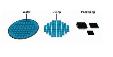
The wafer is produced by Fab, on which chips (die) are placed regularly, and depending on the specific area of the die, hundreds, thousands, or even tens of thousands of chips (die) can be placed on a wafer.
The package Device is the packaged chip, which has many forms according to the final application requirements, and this part is done by the packaging factory in the chip industry value chain.
The basic working mechanism of the test system.

The test machine is programmed to generate any type of signal, multiple signals together to form a test pattern or test vector, apply a test vector to the DUT at a point in the time axis, feed the output generated by the DUT into the instrument of the test machine to measure its parameters, compare the measurement result with the “programmed value” stored in the test machine, if the measurement result matches the “programmed value” in the test machine within acceptable tolerances, then the DUT is considered good, otherwise, it is bad and is recorded according to its type of failure.
Wafer test (or CP-chip probing).
It is the test directly on the wafer in Figure (3), the following figure is a complete wafer test automation system.
Prober — a mechanical device separate from the Tester, the main role is to carry the wafer and let the wafer within a die of each bond pad can be connected to the probe of the probe card, and after the test, remove the previous contact, while moving the wafer, for another die once again connected to the probe card’s probe, and record the test results for each die.

The Probe Card is one of the connection interfaces between the Tester and DUT on the Wafer. The purpose is to connect Tester Channel to the DUT to be tested. Most are tungsten copper or beryllium copper, but also palladium and other materials; Material selection requires high strength, electrical conductivity, and resistance to oxidation, as shown in Figure (5) below.
When the probe card’s probe correctly touches each bond pad of a die in the wafer, it sends a start signal to the tester through the interface to start the test, and the tester sends back the classification signal (End of the test) to the prober when it finishes the test, and the tester and the prober must be connected (docking) to test during mass production.
Final test (FT, or package test) :
The test is performed on the Package Device in Figure (3). The following figure is a complete test system of FT. Compare the wafer test, where the hardware part, prober replaced by the handler, its role is the same, the main role of the handler is the robot arm, grab DUT, placed in the test area, by the tester to test it, and then the handler and then according to the tester test results, grab DUT into the appropriate area, such as good product area, such as bad product 1 category area, bad product 2 category area, etc.

And the probe card is replaced by the load board, its role is similar, but it should be noted that the load board needs to add a device – Socket, which is used to place the packaged device, each different package type needs a different socket, as shown in the following figure (7) shows, the four white devices on the load board are sockets.

The handler must be combined with the tester (this action is called mount machine) and connected to the interface in order to test, the action is the handler’s arm to put the DUT into the socket, then contact the pusher down, so that the DUT’s foot correctly contact with the socket, and then send out the start signal, through the After the test, the tester sends back the binning and EOT signals; the handler does the sorting action.


