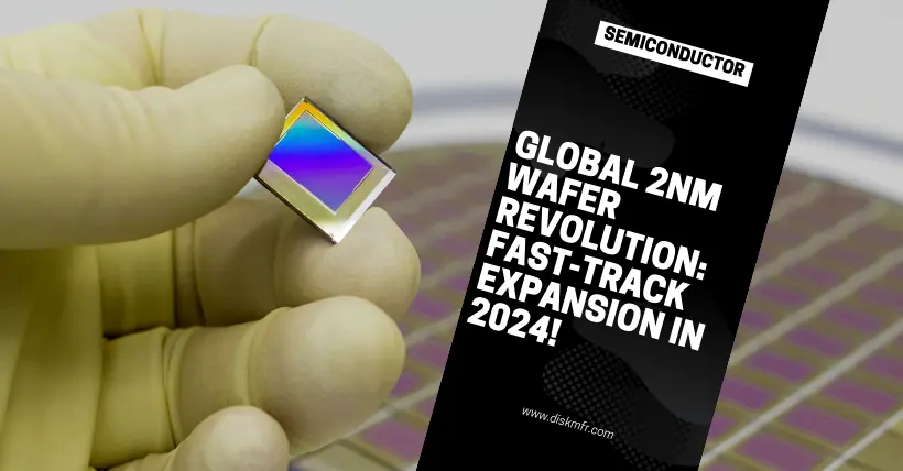
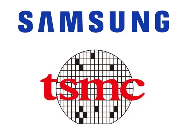
Under the strong push of AI, the importance of advanced process chips is increasingly highlighted. Currently, the 3nm process is the most advanced technology in the industry. Meanwhile, manufacturers such as TSMC, Samsung, Intel, and Rapidus are actively promoting the construction of 2nm wafer fabs. TSMC and Samsung had previously planned to mass-produce 2nm chips by 2025, while Rapidus plans to start trial production of 2nm chips in 2025.
As this timeline approaches, the construction of global 2nm wafer fabs is accelerating.
01
Will the 2nm wafer fab be completed within this year?
Recently, the Semiconductor Industry Association (SEMI) stated that TSMC and Intel are expected to complete the construction of the 2nm wafer fab by the end of this year.
Intel is expected to be the first to commercialize 2nm chips, with its PC CPU Arrow Lake products adopting the 2nm process node. TSMC’s 2nm process is expected to be used in Apple’s iPhone AP chips, and TSMC’s 2nm production capacity is expected to increase significantly.

According to Taiwanese media reports, TSMC is accelerating the installation of equipment for the 2nm process. TSMC’s Baoshan Fab20 P1 plant in Hsinchu plans to install equipment in April this year, start trial production in the second half of the year, and begin small-scale production in the second quarter of 2025.
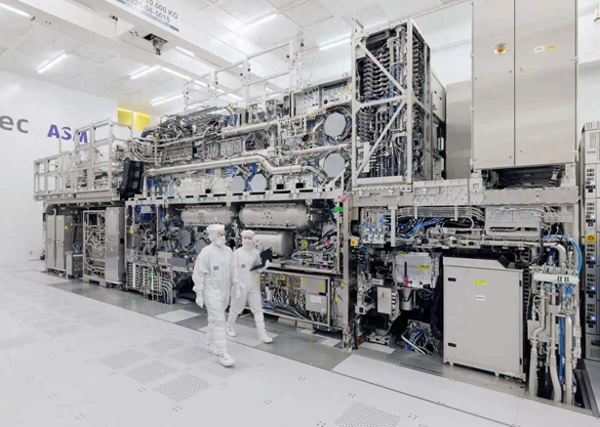
At Intel, ASML delivered the world’s first high numerical aperture High NA EUV EXE:5200 to Intel at the end of last year, aiding in the production of 2nm chips. Intel then began the calibration of the lithography machine, which progressed smoothly.

In February this year, Intel and the ASML technical support team jointly announced that they had activated the light source of the EXE:5000 lithography machine, allowing light to reach the photoresist. This is a crucial step before the lithography machine is fully operational, indicating that the light source is functioning properly. Intel later shared a video showcasing the delivery process of the first high-NA EUV lithography machine, with components being air-freighted from the Netherlands to the USA, reducing delivery time compared to sea freight.
02
Samsung and Rapidus are gearing up
SEMI believes that Samsung may not complete the construction of the 2nm wafer fab this year. However, Samsung’s previously published technology roadmap indicates that it will start mass production of 2nm process chips for mobile devices beginning in 2025, use them in high-performance computing (HPC) products in 2026, and expand to automotive chips in 2027.
As for Rapidus, the company is building a 2nm chip factory in Chitose, Hokkaido, Japan, with the trial production line scheduled to start in April 2025 and mass production targeted for 2027.
Recently, media reports stated that to promote the development of advanced wafer fabs in Japan, several Japanese manufacturers will supply products to Rapidus. Among them, Dai Nippon Printing (DNP) will start mass production of photomasks for 2nm chips in 2027 at its Fukuoka factory and other locations in Japan and supply them to Rapidus. Photomasks are used in the lithography process to form circuits on silicon wafers.
Besides DNP, Japanese company TOPPAN Holdings is also collaborating with IBM to develop photomasks for 2nm, targeting mass production in 2026 and supplying to Rapidus. Additionally, companies like Tokyo Ohka Kogyo (TOK), JSR, and Shin-Etsu Chemical are expected to supply to Rapidus.
03
Plans for 1nm chips revealed!
After 2nm, the next target for wafer fabs is 1nm chips. According to manufacturer plans, the industry expects to see mass production of 1nm-level chips from 2027 to 2030.
TSMC plans to reach the A14 node (1.4nm) by 2027 and the A10 node (1nm) by 2030. Recent media reports state that TSMC intends to set up a factory in Taibao City, Chiayi County, central Taiwan, to produce 1nm chips.
Samsung plans to introduce a 1.4nm process by the end of 2027. The Samsung SF1.4 (1.4 nm) process, which increases the number of nanosheets from three to four, is expected to significantly improve performance and power consumption.
Intel’s latest foundry roadmap shows that the Intel 14A (1.4nm level) node will enter production in 2026, and the Intel 10A (1nm level) will begin development or production by the end of 2027.
04
Conclusion
TrendForce Consulting states that in 2023, due to high inventory in the supply chain, weak global economy, and slow market recovery, the foundry industry was in a downturn, with the top ten foundries’ revenue decreasing by about 13.6% to $111.54 billion. In 2024, driven by AI-related demand, revenue is estimated to increase by 12% to $125.24 billion, with TSMC’s growth rate significantly above the industry average due to stable orders for advanced processes.
Driven by the AI wave, the foundry industry is moving out of the downturn and returning to growth this year, with advanced processes becoming a key driving force. Looking ahead, the competition in advanced process technology in the foundry industry will continue, and after 3nm, who will dominate the 2nm and 1nm era remains to be seen.

Disclaimer: This article is created by the original author. The content of the article represents their personal opinions. Our reposting is for sharing and discussion purposes only and does not imply our endorsement or agreement. If you have any objections, please contact us through the provided channels.


