
Google unveils Google Axion, its first Arm-based processor designed for data centers.
On April 9, Google unveiled Google Axion, its first Arm-based processor designed for the cloud and data centers. In a blog post, Google said Axion is just the latest in the company’s efforts to design its chips, which date back to the first-generation Tensor processor units in 2016, which were also made for Google’s data centers.
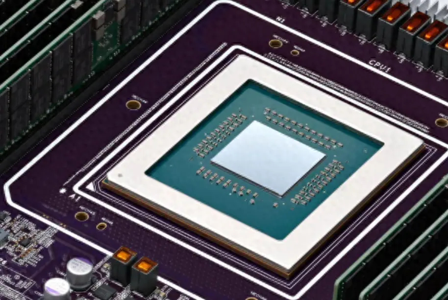
Since the release of the Pixel 6 handset in 2021, Google’s lineup of Pixel smartphones has been using its customized system-on-a-chip (SoC), which is also known as a Tensor. Google claims that the performance of the new Axion chips, which use Arm’s Neoverse V2 platform, will be 30 percent better than the previous Arm-based CPUs made for data centers by 30 percent and by 50 percent over current chips based on x86 designs.
Axion is based on Titanium, a system of dedicated custom silicon microcontrollers and layered scale-out offloads. Titanium offloads platform operations such as networking and security, resulting in greater capacity in Axion processors and improved performance for customer workloads. Hyperdisk is our new block storage service that separates performance from instance size and can be dynamically provisioned in real time.
Google is already using a new generation of Arm-based servers in its data centers to power many of its services, including Google Earth Engine and the YouTube advertising platform, and Google said it will move these and other services to Axion-based servers “soon. Axion-based servers will be available to Google Cloud customers later in 2024. In the meantime, organizations can sign up on Google’s website to fondly try out virtual machines using Axion chips.
Artificial intelligence is one of the hottest topics in technology today and an area where major tech companies are competing to invest. To train a high-performance, highly intelligent AI model requires not only a large amount of data and algorithms but also powerful computing power and hardware support.
In this regard, Google has always been at the forefront. For example, Tensor Processing Units (TPU), chips are optimized to run its TensorFlow software and various machine learning models. For Google, through its expertise and experience in machine learning and TensorFlow software development, its experience with large-scale data centers and cloud infrastructures, it can effectively gain a corresponding advantage in the chip and server market:
To gain more control over the performance, efficiency, and security of their hardware and software stacks.
To reduce dependence on third-party chip suppliers such as Intel and Qualcomm and avoid potential supply chain issues or price volatility.
Enable faster innovation and iteration of their products and services by customizing chips to their specific needs and use cases.
Reduce the cost and complexity of chip design and manufacturing by using machine learning and open-source tools to automate and streamline processes.
Google’s already successful in-house chip projects include:
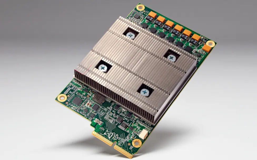
TPU: Google’s customized AI gas pedal that performs matrix multiplication and convolution operations at high speeds with low precision.TPUs are used to train and reason about large-scale neural networks, such as those used for natural language processing, computer vision, and recommender systems.TPUs are available for third-party use through the Google Cloud TPU Service, and can also be sold as smaller versions.
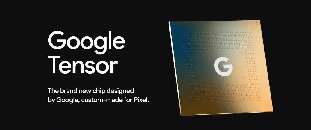
Tensor: Google’s first mobile system-on-a-chip (SoC) designed specifically for the Pixel smartphone. Tensor integrates a soft neural processing unit (NPU) on a field-programmable gate array (FPGA) that accelerates deep neural network inference with low latency and high throughput. Tensor also features a specialized Transformer engine that can solve language models with trillions of parameters.
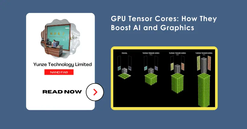
Hopper: Google’s next-generation AI gas pedal based on a new GPU architecture. Hopper features a fourth-generation tensor core and FP8-precision Transformer engine that can speed up large language models by up to 30 times over the previous generation. Hopper also supports the NVLink switching system, which connects up to 256 GPUs to accelerate the scaling of workloads.
Skywater: Google’s open-source project that provides chip designers with software tools for designing, verifying, testing, and fabricating their chips. skywater also offers free access to Skywater Technology Foundry’s 130nm process node for prototyping and production. skywater aims to democratize chip design and reduce the number of hobbyists, scholars, and startups to lower the barrier to entry.
Currently, more than 90% of Google’s AI training work is using these chips, TPUs support the main business of Google, including search, speech recognition, natural language processing, image recognition, and so on. The launch of the new chips means that Google is catching up with Amazon and Microsoft, its competitors in the cloud space. Amazon and Microsoft have already launched ARM-architecture CPUs in 2021 as a way to offer differentiated computing services.


Disclaimer: This article is created by the original author. The content of the article represents their personal opinions. Our reposting is for sharing and discussion purposes only and does not imply our endorsement or agreement. If you have any objections, please contact us through the provided channels.


