Electroplating and electroforming are often confused, but they have distinct purposes and processes. Here’s the difference, as well as the stages in wafer processing where electroplating is used:
01
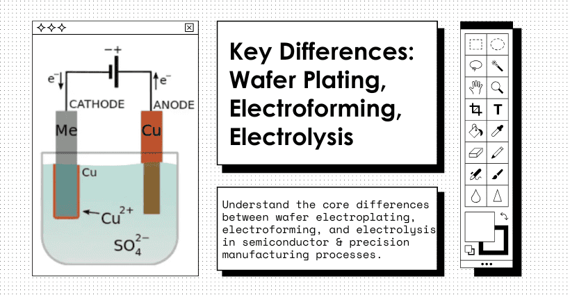
Differences between Electroplating, Electroforming, and Electrolysis
| Process | Electroplating | Electroforming | Electrolysis |
|---|---|---|---|
| Purpose | Depositing a metal layer on a wafer surface (for decoration, corrosion protection, conductivity) | Replicating a mold structure to create a detachable metal part (for structural fabrication) | Decomposing compounds using electric current to purify or produce substances |
| Substrate Retention | Substrate is permanently retained | Mold is usually removed | No substrate needed, only electrolyte |
| Typical Applications | Gold/silver plating, PCB copper plating | Microneedle arrays, electroformed masks, metal micro-molds | Water electrolysis (H₂, O₂ production), copper purification, electrolytic polishing |
| Deposition Location | Wafer surface | Mold surface; structure remains after demolding | Usually involves anode dissolution and gas release |
| Metal Usage | Surface coating for decoration/protection | Precision structural replication | Chemical extraction or decomposition |
Simplified Summary:
- Electroplating: Deposits a thin metal layer on a surface.
- Electroforming: Deposits a thick metal layer, then removes the mold, leaving a freestanding metal structure.
- Electrolysis: Similar in principle but not for depositing metal on the cathode; mainly for decomposition or purification.
02
Electroplating in Wafer Processing
| Application Stage | Electroplated Metals |
|---|---|
| 1. Copper interconnect (Damascene) | Copper (Cu) |
| 2. TSV fill (Through-Silicon Via) | Copper (Cu) |
| 3. Copper pillar process | Nickel/Gold (Ni/Au), Copper (Cu) |
| 4. Solder balls | Tin (Sn), Tin-Silver (SnAg), Gold (Au) |
| 5. RDL (Redistribution Layer) plating | Copper (Cu) |
| 6. MEMS device fabrication | Gold (Au), Copper (Cu), Nickel (Ni) |
| 7. TGV fill | Copper (Cu) |
Related:
- 1g of Silver Nanowire Can Wrap Around Earth 5 Times
- Step-by-Step Guide to Wafer Plating Rate Formula
- Wafer Electroplating: Key Laws You Must Follow Now

Disclaimer:
- This channel does not make any representations or warranties regarding the availability, accuracy, timeliness, effectiveness, or completeness of any information posted. It hereby disclaims any liability or consequences arising from the use of the information.
- This channel is non-commercial and non-profit. The re-posted content does not signify endorsement of its views or responsibility for its authenticity. It does not intend to constitute any other guidance. This channel is not liable for any inaccuracies or errors in the re-posted or published information, directly or indirectly.
- Some data, materials, text, images, etc., used in this channel are sourced from the internet, and all reposts are duly credited to their sources. If you discover any work that infringes on your intellectual property rights or personal legal interests, please contact us, and we will promptly modify or remove it.


