The so-called low numerical aperture EUV remains leading in the industry.
Enthusiastic readers tend to focus on microchips manufactured using cutting-edge process technology, which for Intel means using high numerical aperture extreme ultraviolet (EUV) lithography in the coming years. However, the vast majority of chips we will use in the next few years will be manufactured with low numerical aperture (Low-NA) EUV lithography equipment. This is why ASML’s latest announcement is particularly noteworthy.
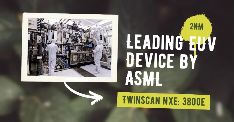
As discovered by Computerbase, ASML delivered its first updated Twinscan NXE: 3800E lithography machine this week for wafer factory installation. The NXE: 3800E is the latest version of the company’s 0.33 numerical aperture (Low-NA) lithography scanner series, designed to manufacture 2nm and 3nm process chips.
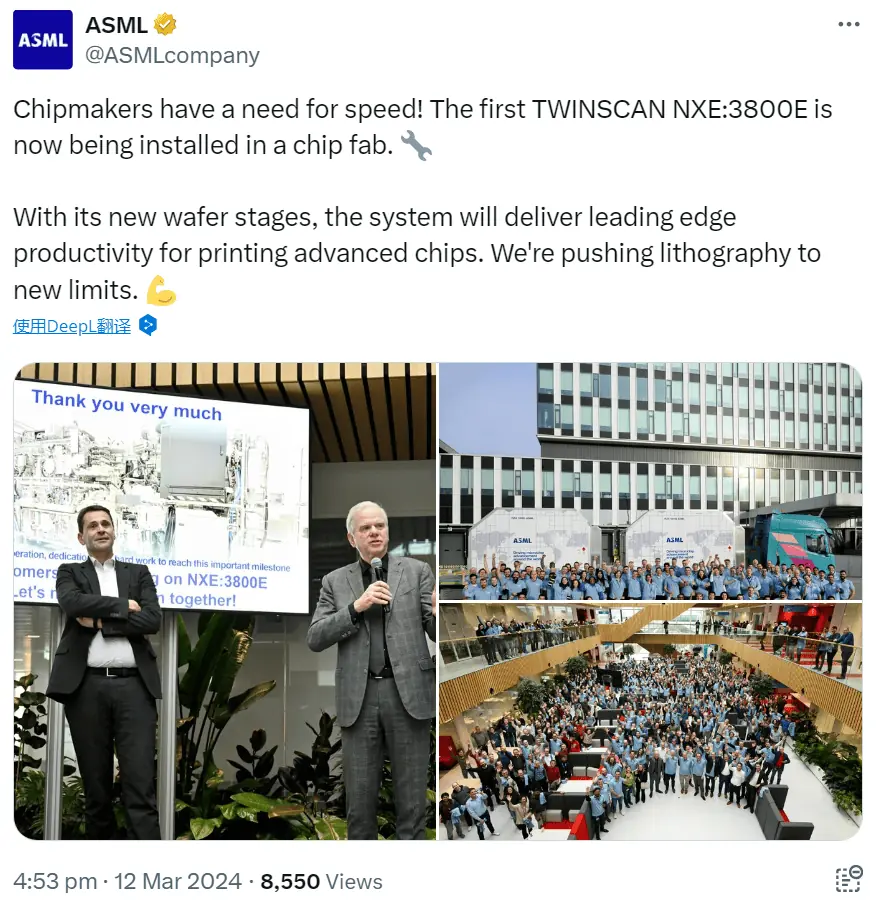
ASML has not yet released all the details about the device’s capabilities, but the company’s previous roadmap indicates that the updated 3800E will offer higher wafer throughput and more accurate wafer alignment, which ASML calls “matching machine coverage.” Based on this roadmap, ASML expects its fifth-generation low numerical aperture EUV scanner to process 200 wafers per hour, marking a significant milestone for the technology, as one of the drawbacks of EUV lithography is its lower throughput compared to today’s well-researched and adjusted deep ultraviolet (DUV) lithography equipment.
For ASML’s logic and memory chip wafer factory customers (currently there are only about six companies in total), the updated scanner will help these wafer factories continue to improve and expand the production of their cutting-edge chips. Even as large wafer factories expand their operations by adding facilities, increasing the output of existing facilities remains an important factor in meeting capacity demands and reducing production costs (or at least controlling production costs).
Since EUV scanners are not cheap—a typical scanner costs about $180 million, and the cost of the Twinscan NXE: 3800E may be higher—these equipment costs need time to be fully amortized. Meanwhile, launching a new generation of EUV scanners faster will have a significant financial impact on ASML, which already enjoys the status of the sole supplier of this critical equipment.
Following the 3800E, ASML has at least one more generation of low numerical aperture EUV scanners in development, including the Twinscan NXE: 4000F, which is expected to be released around 2026.
01
TSMC 3nm capacity is limited, needing stronger EUV.
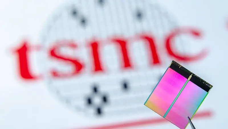
Due to the limitations of equipment and output in TSMC’s 3nm process line, it cannot meet all the needs of Apple’s upcoming new devices.
Brett Simpson, a senior analyst at Arete Research, noted that TSMC’s N3 silicon wafer pricing for Apple will return to normal in the first half of 2024, with an average price of about $16,000 to $17,000. He estimates that TSMC’s current yield for the A17 and M3 processors is about 55%, which aligns with TSMC’s stage of development, with plans to improve the yield by about 5 percentage points each quarter.
Simpson added that TSMC’s focus in the early stages is on optimizing yield and wafer cycle times to improve efficiency.
Mehdi Hosseini, a senior analyst at Susquehanna International Group, said that TSMC’s 3nm process cannot truly ramp up production based on cost considerations until ASML’s new High-NA NXE: 3800E with higher throughput, which requires multiple exposures using ASML’s EUV exposure technology, is launched.
TSMC currently uses ASML’s NXE: 3600D lithography machine system, which can produce 160 wafers per hour (wph).
The NXE: 3800E lithography system can reduce the overall cost of EUV multiple exposures (patterning). Initially, the NXE: 3800E can achieve 30mJ/cm², about 195 wafers per hour, and eventually increase to 220 wafers per hour, a 30% increase in throughput compared to the NXE: 3600D.
02
The $300 million high numerical aperture EUV lithography machine draws attention.
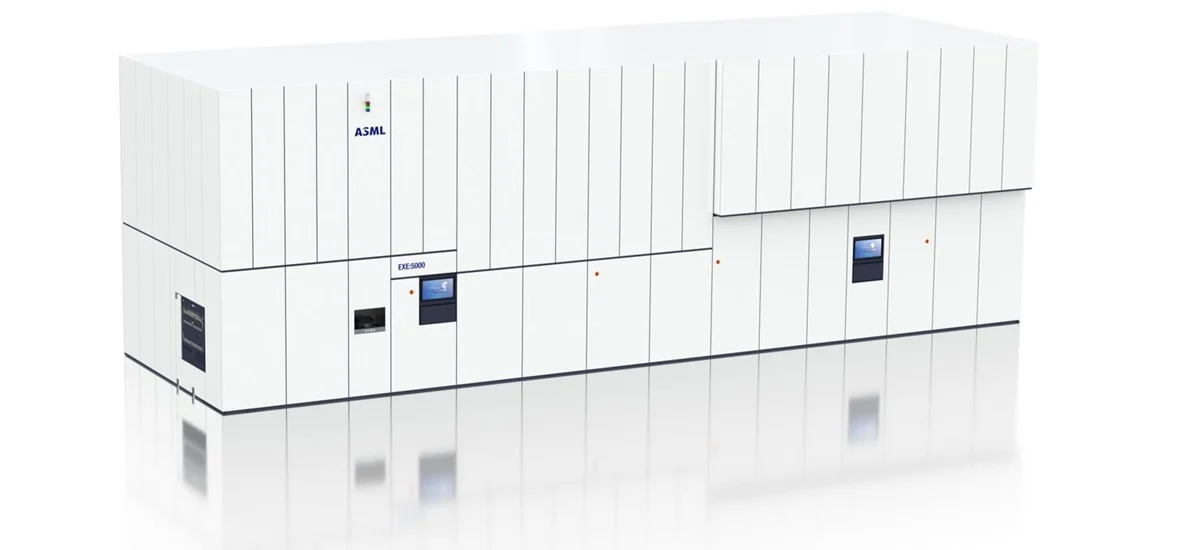
In December last year, ASML delivered the industry’s first EUV lithography equipment with a numerical aperture of 0.55, the Twinscan EXE: 5000, to Intel. Currently, this equipment is primarily used for development purposes and to acquaint the company’s customers with the new technology and its capabilities. The commercial use of high numerical aperture equipment is planned for 2025 and beyond.
Intel announced plans to start using ASML’s high numerical aperture Twinscan EXE scanners for high-volume manufacturing (HVM) starting in 2025 when the company intends to begin using its 18A (1.8nm) process technology. For this, Intel has been experimenting with high numerical aperture lithography equipment since 2018 when it acquired ASML’s Twinscan EXE: 5000. The company has ordered ASML’s next-generation high numerical aperture commercial equipment, the Twinscan EXE: 5200.
High numerical aperture EUV equipment is crucial for higher resolution (<8 nm, current 0.33 NA EUV resolution is 13nm), enabling smaller transistors and higher transistor density. Besides a completely different optical design, high numerical aperture scanners are also expected to provide faster photomask and wafer stages and higher productivity. For example, the Twinscan EXE: 5200’s productivity exceeds 200 wafers per hour (WPH). In comparison, ASML’s top 0.33 NA EUV device, the Twinscan NXE: 3600D, has a WPH of 160.
Intel may use ASML’s high NA tools in its process technology following 18A, while competitors TSMC and Samsung will use them later this decade. These scanners won’t be cheap, with each device’s cost possibly exceeding $300 million, further increasing the cost of the most advanced process wafer fabs.
ASML’s most advanced EUV scanners delivered to customers feature 0.33 NA and 13nm resolution, capable of single exposure patterning of chip features with metal pitches of about 30nm, sufficient for process nodes like 5nm or 4nm. For finer processes, chip manufacturers will either need to use EUV double exposure or patterning techniques, which is what they will be doing in the coming years. Besides this, they plan to use ASML’s next-generation high numerical aperture EUV scanners with a numerical aperture of 0.55 and a resolution of about 8nm.
It’s important to note that the 0.55 NA EUV equipment will not replace the deep ultraviolet (DUV) and EUV devices currently used in wafer fabs, just as the introduction of 0.33 NA EUV did not gradually phase out DUV lithography machines. For the foreseeable future, ASML will continue to advance its DUV and 0.33 NA EUV scanners. At the same time, high numerical aperture EUV lithography technology will continue to play a key role in reducing transistor sizes and enhancing their performance.
Related:
- ASML Targets 0.2nm Tech with Super NA Lithography by 2036!
- ASML’s Massive Investment and 600 Machines: Showdown?

Disclaimer:
- This channel does not make any representations or warranties regarding the availability, accuracy, timeliness, effectiveness, or completeness of any information posted. It hereby disclaims any liability or consequences arising from the use of the information.
- This channel is non-commercial and non-profit. The re-posted content does not signify endorsement of its views or responsibility for its authenticity. It does not intend to constitute any other guidance. This channel is not liable for any inaccuracies or errors in the re-posted or published information, directly or indirectly.
- Some data, materials, text, images, etc., used in this channel are sourced from the internet, and all reposts are duly credited to their sources. If you discover any work that infringes on your intellectual property rights or personal legal interests, please contact us, and we will promptly modify or remove it.


