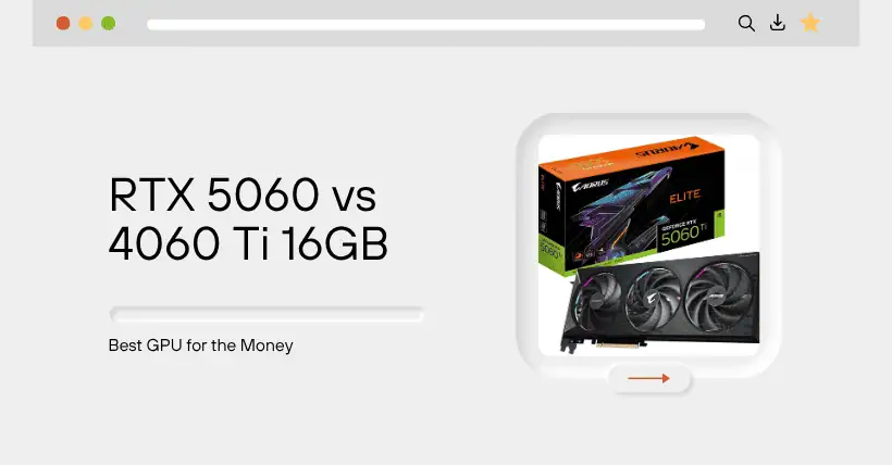
RTX 5060 vs 4060 Ti 16GB: Gaming Test Results
RTX 5060 and 4060 Ti 16GB go head-to-head in real game tests—discover which GPU delivers better performance and value.

RTX 5060 and 4060 Ti 16GB go head-to-head in real game tests—discover which GPU delivers better performance and value.
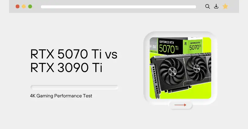
Discover how RTX 5070 Ti stacks against 3090 Ti in 4K gaming with detailed performance insights and benchmark comparisons.

Learn how to select the right crystal for Bluetooth earbuds and avoid common pitfalls with this expert-backed buying guide.

Learn how film agents improve chip cleaners by adding surface protection, increasing efficiency, and enhancing overall cleaning results.
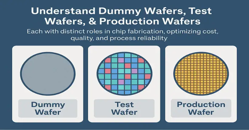
Understand dummy wafers, test wafers, & production wafers—each with distinct roles in chip fabrication, optimizing cost, quality, and process reliability.
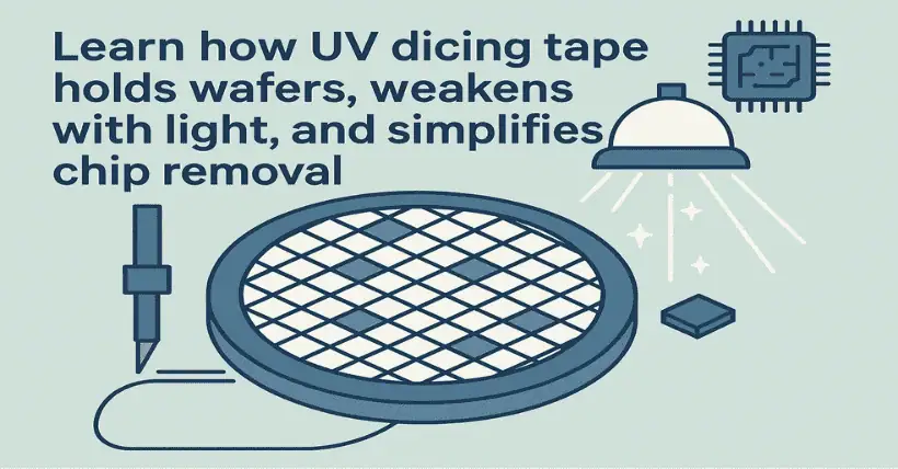
Learn how UV dicing tape holds wafers, weakens with light, and simplifies chip removal after precise semiconductor cutting.

Discover how crystal oscillators work, what drives them, and why the Barkhausen Criterion ensures signal stability in circuits.
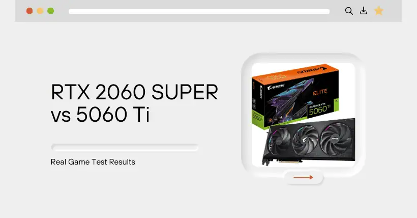
See how the RTX 5060 Ti compares to the 2060 SUPER in real gaming tests—performance gains, frame rates, and upgrade
