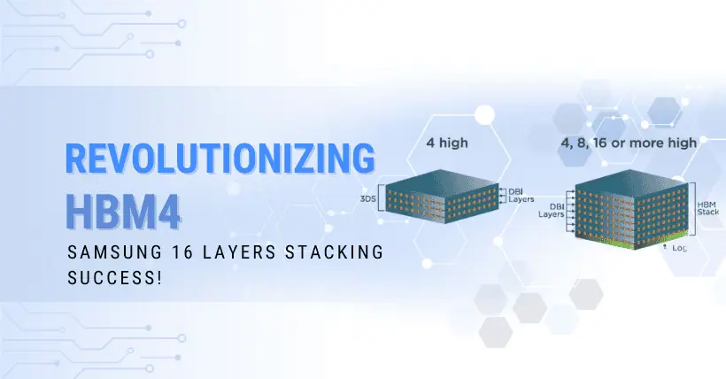
According to South Korean media outlets The Elec and ETNews on April 7th, Dae Woo Kim, an executive from Samsung Electronics’ advanced packaging team, announced during the Korean Microelectronics and Packaging Society’s annual meeting that the company had recently verified a 16-layer hybrid bonding HBM memory technology.
Kim stated that Samsung Electronics has successfully produced a 16-layer stacked HBM3 memory using hybrid bonding technology. This memory sample functions properly and the 16-layer stacked hybrid bonding technology will be utilized for the mass production of HBM4 memory in the future.
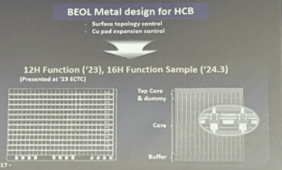
Compared to the current bonding process, hybrid bonding doesn’t require the addition of bumps between DRAM memory layers. Instead, it directly connects the top and bottom layers using copper, which greatly enhances the signal transmission rate and is more suitable for the high bandwidth demands of AI computing.
Hybrid bonding can also decrease the distance between DRAM layers, reducing the overall height of the HMB module. However, it faces challenges such as a lack of maturity and high application costs.
Samsung Electronics is pursuing a dual strategy in HBM4 memory bonding technology, concurrently developing hybrid bonding and the traditional TC-NCF process.
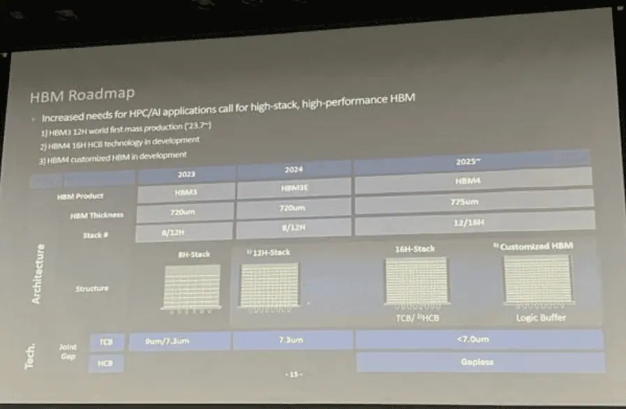
According to the image below and previous reports from DiskMFR, the module height limitation for HBM4 will be increased to 775 micrometers, which is beneficial for the continued use of TC-NCF.
Samsung is working to minimize the wafer gap in the TC-NCF process, aiming to reduce this height to within 7.0 micrometers in HBM4.
Despite skepticism regarding the TC-NCF technology, Kim defended that Samsung Electronics’ solution is more suitable for high-stack modules of 12 layers or even 16 layers, compared to its competitor SK Hynix’s MR-RUF.
Related:

Disclaimer: This article is created by the original author. The content of the article represents their personal opinions. Our reposting is for sharing and discussion purposes only and does not imply our endorsement or agreement. If you have any objections, please contact us through the provided channels.


