HBM competition is becoming increasingly fierce, and Samsung has been forced to yield.
According to five sources, Samsung Electronics plans to use the chip manufacturing technology advocated by its competitor SK Hynix, as the world’s leading memory chip maker seeks to catch up in the race to produce high-end chips that power artificial intelligence (AI).
With the growing popularity of generative AI, the demand for high-bandwidth memory (HBM) chips has surged. However, unlike its peers SK Hynix and Micron Technology, Samsung has been conspicuous in its deal with AI chip leader Nvidia to provide the latest HBM chips.
Analysts and industry observers say one reason for Samsung’s lag is its decision to stick with a chip manufacturing technology known as non-conductive film (NCF), which led to some production issues, while Hynix switched to a mass reflow mold underfill (MR-MUF) method to address the weaknesses of NCF.
However, Samsung recently issued purchase orders for chip manufacturing equipment aimed at handling MUF technology, according to three sources directly familiar with the matter.
“Samsung had to take some measures to increase its HBM production… Adopting MUF technology was somewhat a forced choice for Samsung as it eventually followed the technology first used by SK Hynix,” one of the sources said.
According to several analysts, Samsung’s HBM3 chip yield is about 10% to 20%, while SK Hynix’s HBM3 yield is about 60% to 70%.
HBM3 and HBM3E are the latest versions of HBM chips, and demand for them is strong. They are bundled with core microprocessor chips to help process vast amounts of data in generative AI.
One source said Samsung is also in negotiations with material manufacturers, including Japan’s Nagase, to procure MUF materials. The mass production of high-end chips using MUF is not expected to be ready until next year, as Samsung needs to conduct more testing.
Three sources also stated that Samsung plans to use both NCF and MUF technologies in its latest HBM chips.
Samsung says its internally developed NCF technology is the “optimal solution” for its HBM products and will be used in its new HBM3E chips. “We are proceeding with the HBM3E product business as planned,” Samsung said.
Nvidia and Nagase declined to comment.
Samsung’s plan to use MUF highlights the increasing pressure it faces in the AI chip race. According to data from research firm TrendForce, driven by AI-related demand, the HBM chip market has more than doubled this year, reaching nearly $9 billion.
01
NCF and MUF Technologies
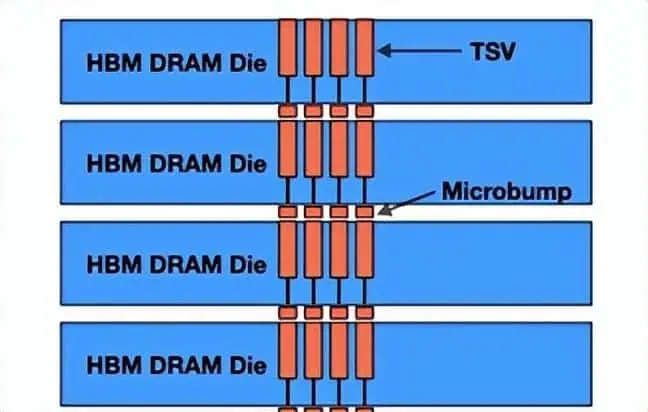
Non-conductive film (NCF) chip manufacturing technology has been widely used by chip manufacturers for stacking multiple layers of chips in compact high-bandwidth memory chipsets, as using thermal compression film helps minimize the space between stacked chips.
However, as more layers are added, manufacturing becomes complex, and there are often issues related to adhesive materials. Samsung states that its latest HBM3E chips have 12 chip layers. Chip manufacturers have been looking for alternatives to address these weaknesses.
SK Hynix took the lead in successfully adopting the Mass Reflow Mold Underfill (MR-MUF) technology, becoming the first supplier to provide HBM3 chips to Nvidia.
Analyst Jeff Kim from KB Securities stated that SK Hynix’s market share in Nvidia’s HBM3 and more advanced HBM products is expected to exceed 80% this year.
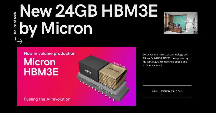
Micron has entered the high-bandwidth memory chip race, announcing its latest HBM3E chips will be adopted by Nvidia to power the latter’s H200 Tensor chip, which will start shipping in the second quarter.
Samsung’s HBM3 series has not yet passed Nvidia’s supply deal qualification, as revealed by one of the four sources and another informed individual. The setback Samsung is facing in the AI chip race has also caught investors’ attention, with its stock price falling 7% this year, trailing behind SK Hynix and Micron, which have risen by 17% and 14%, respectively.
02
SK Hynix Continues to Advance
Hoyoung Son, SK Hynix’s senior manager of advanced packaging development, stated, “Developing customer-specific AI memory requires a new approach, as the technology’s flexibility and scalability become crucial.”

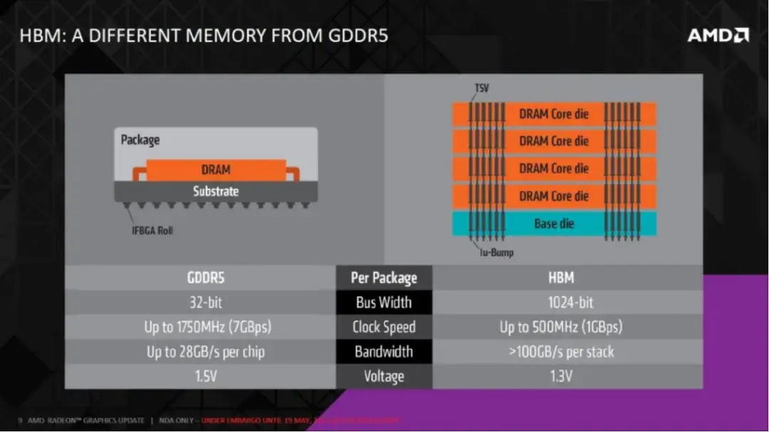
In terms of performance, HBM memory with a 1024-bit interface has evolved rapidly: from a 1GT/s data transfer rate in 2014–2015 to the recently introduced HBM3E memory devices reaching 9.2 GT/s – 10 GT/s. With HBM4, the memory is set to transition to a 2048-bit interface, ensuring a steady bandwidth increase over HBM3E.
However, according to Hoyoung Son, some clients might benefit from differentiated (or semi-custom) solutions based on HBM.
“To realize diversified AI, the characteristics of AI memory also need to become more diverse,” Hoyoung Son said in an interview with BusinessKorea, “Our goal is to have a variety of advanced packaging technologies that can cope with these changes. We plan to offer differentiated solutions that can meet any customer need.”
For the 2048-bit interface, many HBM4 solutions might be custom or at least semi-custom, based on the official and unofficial information we have about the upcoming standards. Some clients might prefer to continue using interposer layers (which will become very expensive), while others might opt for direct bonding techniques to mount HBM4 modules directly onto logic chips, which is also costly.
Manufacturing differentiated HBM products requires complex packaging technologies, including (but not limited to) SK Hynix’s MR-MUF technology. Given the company’s extensive experience in HBM, it is likely to come up with something else, especially for differentiated products.
“Our goal is to have a range of advanced packaging technologies to address the constantly changing technology landscape. Looking ahead, we plan to offer differentiated solutions to meet the needs of all customers,” said Hoyoung Son.
| Category | HBM1 | HBM2 | HBM2E | HBM3 | HBM3E |
|---|---|---|---|---|---|
| BW (GB/s) | 128 | 307 | 460 | 819 | 1000 |
| Stack Height (Layer) | 4 | 4/8 | 4/8 | 8/12 | 8/12 |
| Capacity (GB) | 1 | 4/8 | 8/16 | 16/24 | 24/36 |
| I/O (Gbps) | 1 | 2.4 | 3.6 | 6.4 | 8.0 |
| JEDEC Release Date | Jan. 2016 | Dec. 2018 | Feb. 2020 | Jan. 2022 | Aug. 2023 |
| Channels | 8 | 8 | 12 | 16 | 16 |
| Storage number per channel | 128MB | 1GB | 1GB | 1.5GB | TBD |
| Process node | 29nm | 21nm | 10nm | 5nm | 10nm |
| Effective bit width | 1024-bit | 1024-bit | 1024-bit | 1024-bit | 1024-bit |
| Voltage | 1.2 | 1.2 | 1.2 | 1.1 | TBD |
| Transfer Speed | 1GT/sec/pin | 2GT/sec/pin | 3.2GT/sec/pin 3.65GT/sec/pin | 6.4GT/sec/pin 6.4GT/s | 8GT/s |
| Total channel width | 1024 bits (8-Hi stack) | 1024 bits (8-Hi stack) | 1024 bits (8-Hi stack) | 1024 bits (8-Hi stack) | 1024 bits (8-Hi stack) |
Related:
- Kioxia & SK Hynix Unite: Manufacturing Powerhouse Emerges
- Record R&D by Korean Storage Firms Amid Downturn

Disclaimer:
- This channel does not make any representations or warranties regarding the availability, accuracy, timeliness, effectiveness, or completeness of any information posted. It hereby disclaims any liability or consequences arising from the use of the information.
- This channel is non-commercial and non-profit. The re-posted content does not signify endorsement of its views or responsibility for its authenticity. It does not intend to constitute any other guidance. This channel is not liable for any inaccuracies or errors in the re-posted or published information, directly or indirectly.
- Some data, materials, text, images, etc., used in this channel are sourced from the internet, and all reposts are duly credited to their sources. If you discover any work that infringes on your intellectual property rights or personal legal interests, please contact us, and we will promptly modify or remove it.


