Before introducing the Bevel Etch process, a brief overview of the thin film process: Chemical Vapor Deposition (CVD) is a process in which a layer of solid film is deposited on the surface of a silicon wafer through a chemical reaction of mixed gases. The surface of the silicon wafer and the adjacent areas are heated to provide additional energy to the reaction system. When compounds are mixed and react in the reaction chamber, the CVD process occurs. Atoms or molecules are deposited on the silicon wafer surface to form a film.
During the film deposition process, reaction gases can enter the backside of the wafer through the gaps between the wafer edges and the equipment hardware. After deposition, in addition to the front side, a layer of film also grows on the wafer’s edges and backside. Due to the decreasing concentration of reaction gases from the front side to the edge and then to the backside, the corresponding film thickness also gradually decreases. The film on the side and back of the wafer has poor uniformity. The film thickness accumulates gradually during the wafer production process and constantly contacts or collides with the equipment hardware during transportation, often becoming a potential source of defects.
Consequences of edge flaking defects:
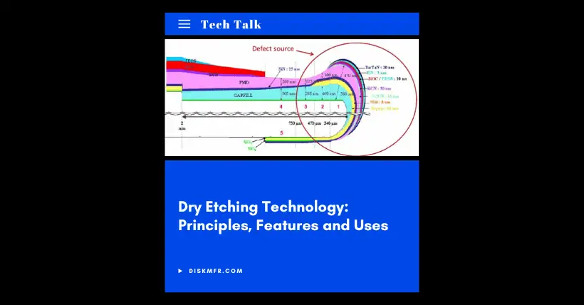
Defect detection during the film growth process has revealed flaking defects distributed in specific locations. These defects are concentrated on the wafer edge, with defect sizes larger than 1 µm. Station-by-station observations show that these defects cause copper wiring disconnection after CMP, leading to device failure.
Furthermore, studies have found that the number of defects worsens as the number of metal layers increases:
The semiconductor bevel process is a processing technique for the edges of semiconductor wafers, mainly used to eliminate defects and surface roughness at the wafer edge, thereby improving wafer processing quality and yield. In semiconductor manufacturing, defects and surface roughness at the wafer edge directly affect the effectiveness of subsequent processes and device performance. Therefore, the semiconductor bevel process plays a very important role in semiconductor manufacturing.
Etching method introduction:
Wet etching: Uses chemical solutions (such as HF to remove oxide layers, H₃PO₄ to etch silicon nitride) to locally spray the edge. It has a short reaction time and low cost, but requires strict temperature control and waste liquid treatment.
Dry etching: Uses plasma (such as CF₄/O₂ gases) to directionally bombard the edge, offering high anisotropy and less contamination, but the equipment is complex and costly. By selecting and combining various etching gases, the bevel etching process can fully cover multiple types of film materials such as PR (photoresist), OX (oxide), SiN (silicon nitride), Carbon, and Metal. N₂ is used to protect areas that do not require etching, preventing etching gases from penetrating.
As the technology nodes of the integrated circuit industry continue to evolve, improving chip yield presents increasingly stringent challenges. The substantial increase in process steps, along with the surge in defects caused by by-products and residues deposited at wafer edges, has become a serious threat to product yield. Consequently, more manufacturers in fields such as logic and memory chips are focusing on the 1 mm edge area of 12-inch wafers, aiming to improve chip yield from the wafer’s edge. Bevel etching tools, as a strong guarantee for yield improvement in the industry, are becoming increasingly important.
Laser etching (emerging technology): Uses high-energy lasers to directly ablate edge materials, offering high precision and no chemical pollution, but has not yet been widely applied.
Outlook:
In the future, as semiconductor technology continues to develop, the performance requirements for semiconductor devices will become increasingly demanding, which will place higher demands on the semiconductor bevel process. To meet the ever-growing performance requirements of semiconductor devices, the future semiconductor bevel process must continue to undergo technological upgrades and innovations, further improving processing accuracy, reducing costs, and increasing yield.
Related:

Disclaimer:
- This channel does not make any representations or warranties regarding the availability, accuracy, timeliness, effectiveness, or completeness of any information posted. It hereby disclaims any liability or consequences arising from the use of the information.
- This channel is non-commercial and non-profit. The re-posted content does not signify endorsement of its views or responsibility for its authenticity. It does not intend to constitute any other guidance. This channel is not liable for any inaccuracies or errors in the re-posted or published information, directly or indirectly.
- Some data, materials, text, images, etc., used in this channel are sourced from the internet, and all reposts are duly credited to their sources. If you discover any work that infringes on your intellectual property rights or personal legal interests, please contact us, and we will promptly modify or remove it.


